From WikiChip
Difference between revisions of "arm holdings/microarchitectures/cortex-a7"
| (4 intermediate revisions by the same user not shown) | |||
| Line 8: | Line 8: | ||
|process=40 nm | |process=40 nm | ||
|process 2=28 nm | |process 2=28 nm | ||
| + | |isa=ARMv7 | ||
|predecessor=Cortex-A9 | |predecessor=Cortex-A9 | ||
|predecessor link=arm_holdings/microarchitectures/cortex-a9 | |predecessor link=arm_holdings/microarchitectures/cortex-a9 | ||
| Line 17: | Line 18: | ||
== Architecture == | == Architecture == | ||
=== Key changes from {{\\|Cortex-A9}} === | === Key changes from {{\\|Cortex-A9}} === | ||
| − | {{ | + | * [[28 nm process]] (from [[40 nm]]) |
| + | * New [[in-order]] pipeline (form [[out-of-order]]) | ||
| + | ** Shorter [[pipeline]] (8, down from 9-12) | ||
| + | *** 0.5x frequency (1 GHz, down from 2 GHz) | ||
| + | * Integer | ||
| + | ** Hardware [[division]] support | ||
| + | ** Hardware [[Fused Multiply-Accumulate]] | ||
| + | * [[VFPv4]] (from [[VFPv3]]) | ||
| + | * [[NEONv2]] (from [[NEON]]) | ||
| + | * Memory subsystem | ||
| + | ** Level 1 [[instruction cache]] reduced to 2-way set associative (down from 4-way) | ||
| + | ** Added {{arm|LPAE}} support | ||
| + | |||
| + | {{expand list}} | ||
| + | |||
=== Block Diagram === | === Block Diagram === | ||
{{empty section}} | {{empty section}} | ||
| Line 36: | Line 51: | ||
* [[Samsung]] | * [[Samsung]] | ||
* [[STEricsson]] | * [[STEricsson]] | ||
| − | * [[Texas | + | * [[Texas Instruments]] |
| − | |||
}} | }} | ||
Latest revision as of 14:24, 31 December 2018
| Edit Values | |
| Cortex-A7 µarch | |
| General Info | |
| Arch Type | CPU |
| Designer | ARM Holdings |
| Manufacturer | TSMC |
| Introduction | October 19, 2011 |
| Process | 40 nm, 28 nm |
| Instructions | |
| ISA | ARMv7 |
| Succession | |
Cortex-A7 (codename Kingfisher) is the successor to the Cortex-A9, a high efficiency ARM microarchitecture designed by ARM Holdings for the mobile market. This microarchitecture is designed as a synthesizable IP core and is sold to other semiconductor companies to be implemented in their own chips. The Cortex-A7 was introduced along with the big.LITTLE technology so that it could be integrated along with the a higher-performance core such as the Cortex-A15 or the Cortex-A17 for better energy and power efficiency.
Contents
Architecture[edit]
Key changes from Cortex-A9[edit]
- 28 nm process (from 40 nm)
- New in-order pipeline (form out-of-order)
- Shorter pipeline (8, down from 9-12)
- 0.5x frequency (1 GHz, down from 2 GHz)
- Shorter pipeline (8, down from 9-12)
- Integer
- Hardware division support
- Hardware Fused Multiply-Accumulate
- VFPv4 (from VFPv3)
- NEONv2 (from NEON)
- Memory subsystem
- Level 1 instruction cache reduced to 2-way set associative (down from 4-way)
- Added LPAE support
This list is incomplete; you can help by expanding it.
Block Diagram[edit]
| This section is empty; you can help add the missing info by editing this page. |
Memory Hierarchy[edit]
| This section is empty; you can help add the missing info by editing this page. |
Licensees[edit]
Arm named the following companies as licensees.
Die[edit]
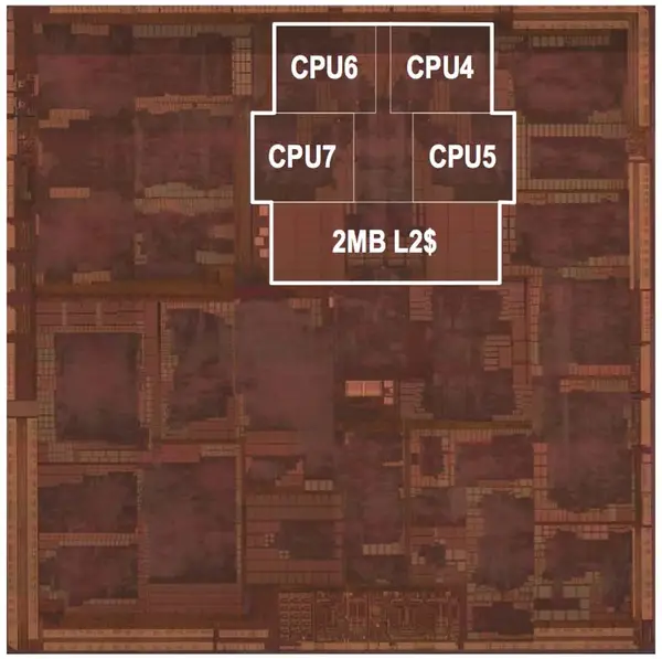
MediaTek MT6595[edit]
- TSMC 28 nm process
- 89 mm² die size
- Quad-core Cortex-A7
- ~0.48 mm² per core
- Quad-core Cortex-A17 + 2 MiB L2
- ~1.93 mm² per core
- ~3.93 mm² for 2 MiB L2
(small quad-core is unlabeled below the big core cluster)
Bibliography[edit]
- Mair, Hugh, et al. "23.3 A highly integrated smartphone SoC featuring a 2.5 GHz octa-core CPU with advanced high-performance and low-power techniques." Solid-State Circuits Conference-(ISSCC), 2015 IEEE International. IEEE, 2015.
Facts about "Cortex-A7 - Microarchitectures - ARM"
| codename | Cortex-A7 + |
| designer | ARM Holdings + |
| first launched | October 19, 2011 + |
| full page name | arm holdings/microarchitectures/cortex-a7 + |
| instance of | microarchitecture + |
| instruction set architecture | ARMv7 + |
| manufacturer | TSMC + |
| microarchitecture type | CPU + |
| name | Cortex-A7 + |
| process | 40 nm (0.04 μm, 4.0e-5 mm) + and 28 nm (0.028 μm, 2.8e-5 mm) + |
