(→Memory Subsystem) |
(→Codenames) |
||
| Line 65: | Line 65: | ||
! Chipset !! Platform !! PHC !! Core !! Target | ! Chipset !! Platform !! PHC !! Core !! Target | ||
|- | |- | ||
| − | | {{intel|Poulsbo|l=chipset}} || {{intel|Menlow}} || || {{intel|Silverthorne}} || MIDs | + | | {{intel|Poulsbo|l=chipset}} || {{intel|Menlow}} || || {{intel|Silverthorne|l=core}} || MIDs |
|- | |- | ||
| − | | {{intel|Poulsbo|l=chipset}} || {{intel|Menlow}} || || {{intel|Diamondville}} || Nettops | + | | {{intel|Poulsbo|l=chipset}} || {{intel|Menlow}} || || {{intel|Diamondville|l=core}} || Nettops |
|- | |- | ||
| − | | || {{intel|Moorestown}} || {{intel|Langwell}} || {{intel|Lincroft}} || MIDs | + | | || {{intel|Moorestown}} || {{intel|Langwell}} || {{intel|Lincroft|l=core}} || MIDs |
|- | |- | ||
| − | | || {{intel|Pine Trail}} || {{intel|Tiger Point}} || {{intel|Pineview}} || Nettops | + | | || {{intel|Pine Trail}} || {{intel|Tiger Point}} || {{intel|Pineview|l=core}} || Nettops |
|- | |- | ||
| − | | || {{intel|Queens Bay}} || {{intel|Topcliff}} || {{intel|Tunnel Creek}} || Embedded | + | | || {{intel|Queens Bay}} || {{intel|Topcliff}} || {{intel|Tunnel Creek|l=core}} || Embedded |
|- | |- | ||
| − | | || {{intel|Queens Bay}} || {{intel|Topcliff}} || {{intel|Stellarton}} || Embedded + [[Altera]] FPGA | + | | || {{intel|Queens Bay}} || {{intel|Topcliff}} || {{intel|Stellarton|l=core}} || Embedded + [[Altera]] FPGA |
|- | |- | ||
| || || || {{intel|Sodaville}} || CE | | || || || {{intel|Sodaville}} || CE | ||
| Line 87: | Line 87: | ||
! First Generation !! !! Second Generation | ! First Generation !! !! Second Generation | ||
|- | |- | ||
| − | | {{intel|Silverthorne}} || → || {{intel|Lincroft}} | + | | {{intel|Silverthorne|l=core}} || → || {{intel|Lincroft}} |
|- | |- | ||
| − | | {{intel|Diamondville}} || → || {{intel|Pineview}} | + | | {{intel|Diamondville|l=core}} || → || {{intel|Pineview}} |
|- | |- | ||
| || || {{intel|Tunnel Creek}} | | || || {{intel|Tunnel Creek}} | ||
| Line 99: | Line 99: | ||
| || || {{intel|Groveland}} | | || || {{intel|Groveland}} | ||
|} | |} | ||
| + | |||
== Release Dates == | == Release Dates == | ||
The {{intel|Atom}} family was officially announced on March 2, 2008 under the '''Intel Atom''' and '''Intel Centrino Atom''' brands. Bonnell was first introduced on April 2nd [[2008]] during the Intel Developers Forum in Shanghai. | The {{intel|Atom}} family was officially announced on March 2, 2008 under the '''Intel Atom''' and '''Intel Centrino Atom''' brands. Bonnell was first introduced on April 2nd [[2008]] during the Intel Developers Forum in Shanghai. | ||
Revision as of 06:05, 27 March 2017
| Edit Values | |
| Bonnell µarch | |
| General Info | |
| Arch Type | CPU |
| Designer | Intel |
| Manufacturer | Intel |
| Introduction | March 2, 2008 |
| Phase-out | 2011 |
| Process | 45 nm |
| Core Configs | 1, 2 |
| Pipeline | |
| Type | Superscalar |
| Speculative | No |
| Reg Renaming | No |
| Stages | 16-19 |
| Instructions | |
| ISA | IA-32, x86-64 |
| Extensions | MOVBE, MMX, SSE, SSE2, SSE3, SSSE3 |
| Cache | |
| L1I Cache | 32 KiB/Core 8-way set associative |
| L1D Cache | 24 KiB/Core 6-way set associative |
| L2 Cache | 512 KiB/Core 8-way set associative |
| Cores | |
| Core Names | Silverthorne, Diamondville, Lincroft, Pineview, Tunnel Creek, Stellarton, Sodaville, Groveland |
| Succession | |
Bonnell was a microarchitecture for Intel's 45 nm ultra-low power microprocessors first introduced in 2008 for their then-new Atom family. Bonnell, which was named after the highest point in Austin - Mount Bonnell, was Intel's first x86-compatible microarchitecture designed to target the ultra-low power market.
Bonnell (project Silverthorne then) was designed by a then-new low-power design team Intel created at their Texas Development Center in Austin in 2004 along with a new chipset (Poulsbo) design team. The design team was led by Elinora Yoeli. While Yoeli previously worked at her native country, Bonnell was a US design and was unconnected to any of Intel's projects worked on by the Israel Design Center in Haifa. Previously Yoeli led the Israeli team in the development of Pentium M.
Contents
Codenames
| Chipset | Platform | PHC | Core | Target |
|---|---|---|---|---|
| Poulsbo | Menlow | Silverthorne | MIDs | |
| Poulsbo | Menlow | Diamondville | Nettops | |
| Moorestown | Langwell | Lincroft | MIDs | |
| Pine Trail | Tiger Point | Pineview | Nettops | |
| Queens Bay | Topcliff | Tunnel Creek | Embedded | |
| Queens Bay | Topcliff | Stellarton | Embedded + Altera FPGA | |
| Sodaville | CE | |||
| Groveland | CE |
Generation successor
| First Generation | Second Generation | |
|---|---|---|
| Silverthorne | → | Lincroft |
| Diamondville | → | Pineview |
| Tunnel Creek | ||
| Stellarton | ||
| Sodaville | ||
| Groveland |
Release Dates
The Atom family was officially announced on March 2, 2008 under the Intel Atom and Intel Centrino Atom brands. Bonnell was first introduced on April 2nd 2008 during the Intel Developers Forum in Shanghai.
Process Technology
| 45 nm Manufacturing Fabs | |
|---|---|
| Fab | Location |
| D1D | Hillsboro, Oregon |
| Fab 32 | Chandler, Arizona |
| Fab 28 | Kiryat Gat, Israel |
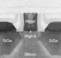
Bonell is designed to be manufactured using a 45 nm process. Intel's 45 nm process is the first high-volume manufacturing process to introduce High-k + metal gate transistors.
| Bonnell | |
|---|---|
| 45 nm | |
| Gate Pitch | 180 nm |
| Interconnect Pitch | 160 nm |
| SRAM bit cell (HD) | 0.346 µm² |
| SRAM bit cell (LP) | 0.3816 µm² |
Compiler support
| Compiler | Arch-Specific | Arch-Favorable |
|---|---|---|
| GCC | -march=bonnell |
-mtune=bonnell
|
| LLVM | -march=bonnell |
-mtune=bonnell
|
| Visual Studio | /arch:SSE3
|
Architecture
Bonnell features a brand new architecture not based on any previous Intel design. The architecture was specifically designed for ultra-mobile PCs (UMPCs), mobile internet devices (MID), and other embedded devices. Bonnell's primary goals were:
- Reduce power consumption,
- while staying fully x86-compatible,
- at acceptable performance
Performance/Power new rule: +1% performance for at most +1% power consumption.
Architecture
- Strictly ultra-low power
- 45 nm process, 9 metal layers, CMOS
- 500 mW to 2 W TDP
- Average 220 mW
- Idle under 80 mW
- 533 MT/s dual mode (GTL & CMOS) FSB
- In-order
- 2-issue decode
- Simple 2-way SMT
- Instruction Queue of 32 entries (16 entries/thread)
- FP Register File (per thread)
- Integer Register File (per thread)
- Private L1 cache for each core
- Shared L2 cache for the entire chip
The number of functional units were kept to minimum to cut on power consumption.
- 2 address generation units (AGUs)
- 2 Integer ALUs (1 for jumps, 1 for shifts)
- 2 FP ALUs (1 adder, 1 for others)
- No Integer multiplier & divider (shared with FP ALU instead)
Memory Hierarchy
- Cache
- Hardware prefetchers
- C6 cache
- 10.5 KiB array to hold the architectural state during deep power down state
- 1-read, 1-write ported
- L1 Instruction Cache
- 36 KiB
- 32 KiB Instruction + 4 KiB Boundary Mark
- 8-way set associative
- 1 read and 1 write port
- 8 transistors (instead of 6) to reduce voltage
- 1-bit pairty (but no ECC)
- 36 KiB
- L1 Data Cache
- 24 KiB
- 6-way set associative
- 1 read and 1 write port
- 8 transistors (instead of 6) to reduce voltage
- 1-bit pairty (but no ECC)
- Per core
- 24 KiB
- L2 Cache:
- 512 KiB 8-way set associative
- ECC support
- Shrinkable from 512 KiB to 128 KiB (2-way)
- 64-bit cache line
- Per core
- Tag/LRU/State bit
- All in one array
- Tag + data = 4.5 KiB + 17.5 KiB
- L3 Cache:
- No level 3 cache
- RAM
- Maximum of 2 GiB, 4 GiB, and 8 GiB
Note that the L1 cache for data and instructions were originally both 32 KiB (8-way), however due to power restrictions, the L1d$ was later reduced to 24 KiB.
- TLB
- ITLB
- 32-entry
- fully associative
- DTLB
- 4 KiB PAges
- 64-entry TLB
- 4-way set associative
- 16-entry micro-TLB
- fully associative
- duplicated for each thread
- 16-entry PDE cache
- fully associative
- 64-entry TLB
- Large Pages
- 8 entries, 4-way set associative
- 4 KiB PAges
- ITLB
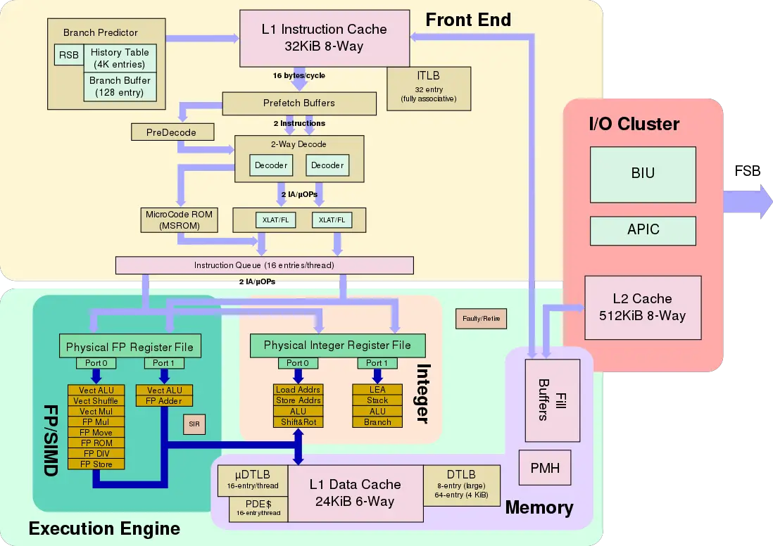
Block Diagram
Overview
Bonnell's architecture shares very little in common with other Intel designs. To achieve the strict ultra-low power objects, Bonnell features a very slimmed own design discarding many high-performance techniques used by Intel's high-performance architectures such as aggressive speculative execution, out-of-order execution, and µop transformation.
Part of the design requirement was that Bonnell retain full x86 compatibility, up to the latest extension - at the 10th of the power consumption of the Pentium M. This meant any software is now 100% compatible but it forced engineers to deal with all the baggage the architecture brought along. The decision to offer full compatibility brought its own set of benefits such as access to the largest software code base in the world, including the ability to run any other x86 operating system unmodified. At the same time it forced the design team to resort to other means of reducing power.
Up to Bonnell, all of Intel's existing architectures put very low priority on power efficiency (note that this has significantly changed since the introduction of Sandy Bridge). High-performance, high-throughput, complex designs are simply inadequate for the kind of power goals required out of Bonnell, even if they were trimmed down. It was decided that Bonnel would be designed from the scratch with power goals in mind. For those reasons Bonnell resembles the P5 microarchitecture.
Pipeline
Much like the original P5 microarchitecture, Bonnell consists of an in-order dual-issue pipeline. The pipeline is shown below. Note the pipeline is duplicated for dual-issue execution.
Unlike P5, which only had 5 stages, Bonnell has 16 to 19 stages pipeline. The longer pipeline allows a more evenly spreading of heat across the chip with more units. This also allows a higher clock rate.
Front End
Bonnell's front end is very simple when compared to Intel's high-performance architectures. Out-of-order execution (OoOE) that is found ubiquitously in all HPC architectures was rejected. Bonnell's power and area constraints simply couldn't allow for the complex logic needed to support that capability. The Instruction Fetch consists of 3 stages capable going through up to 16 bytes per cycle. Like fetch, the Instruction Decode is also 3 stages capable of decording instructions with up to 3 prefixes each cycle (considerably longer for more complex instructions).
Bonnell is a departure from all modern x86 architectures with respect to decoding (including those developed by AMD and VIA and every Intel architecture since P6). Whereas modern architectures transform complex x86 instructions into a more easily digestible µop form, Bonnell does almost no such transformations. The pipeline is tailored to execute regular x86 instructions as single atomic operations consisting of a single destination register and up to three source-registers (typical load-operate-store format). Most instructions actually correspond very closely to the original x86 instructions. This design choice results in lower complexity but at the cost of performance reduction. Bonnell has two identical decoders capable of decoding complex x86 instructions. Being variable length instruction architecture introduces an additional layer of complexity. To assist the decoders, Bonnell implements predecoders that determine instruction boundaries and mark them using a single-bit marker. Two cycles are allocated for predecoding as well as L1 storage. Boundary marks are also stored in the L1 eliminating the need to preform needlessly redundant predecoding. Repeated operations are retrieved pre-marked eliminating two cycles. Bonnel has a 36 KiB L1 instruction cache consisting of 32 KiB instruction cache and 4 KiB instruction boundary mark cache. All instructions (coming from both cache or predecode) must undergo full decode. It's worthwhile noting that Intel states Bonnell is a 16-stage pipeline because for the most part, after a cache hit you'll have 16 stages. This is also true in some cases where the processor can simultaneously decode the next instruction. However, in the cases where you get a miss, it will cost 3 additional stages to catch up and locate the boundary for that instruction for a total of 19 stages.
Some x86 instructions are simply too complex to handle directly. Those selected few get diverted into the microcode sequencer for decoding producing much more sane RISCish instructions at the cost of 2 additional cycles. Intel estimates that only 5% of common software require instructions to be split up. The inability to execute things out-of-order eliminates lots of optimization opportunities at this stage. One thing Bonnell can do is lockstep instructions that can be execute simultaneously such as in the case of instructions that performance a memory access along an arithmetic operation. In those instances Bonnell will issue the instruction as if it were two separate instructions executing simultaneously.
Because Bonnell has support for Hyper-Threading, Intel's brand name for their own simultaneous multithreading technology, a number of modifications had to be done. The prefetch buffer and the instruction queue have been duplicated for each thread.
Branch predictor
No aggressive speculative execution is done in Bonnell, however it does implements a light-weight Gshare branch predictor consisting of a two-level adaptive predictor with a 12-bit global history table. The pattern history table has 4096 entries and is competitively shared between threads. The branch buffer target has 128 entries (4-way by 32 sets). While unconditional jumps are not recorded in the table, always-taken and never-taken jumps do.
The branch-misprediction penalty is 11 to 13 cycles. Some of the rare or complex x86 instructions will detour into a microcode sequencer for decoding, necessitating two additional clock cycles. Additionally there is a roughly 7 cycle penalty for correctly predicted branches but no target can be predicted because of a missing branch target buffer (BTB) entry. Bonnell return stack buffer is 8-entry deep.
Back End
Each cycle two instructions are dispatched in-order. The scheduler can take a pair of instructions from a single thread or across threads. Bonnell in-order back-end resembles a traditional early 90s design featuring a dual ALU, a dual FPU and a dual AGU. Similarly to the front-end, in order to accommodate simultaneous multithreading, the Bonnell design team chose to duplicate both the floating-point and integer register files. The duplication of the register files allows Bonnell to perform context switching on each stage by maintaining duplicate states for each thread. The decision to duplicate this logic directly results in more transistors and larger area of the silicon. Overall implementing SMT still required less power and less die area than the other heavyweight alternatives (i.e., out-of-order and larger superscaler). Nonetheless the total register file area accounts for 50% of the entire core's die area which was single-handedly an important contributor to the overall chip power consumption.
FP/SIMD execution Cluster
In the further pursuit of power saving specialized execution units were minimized as much as possible. Bonnell's floating point & SIMD execution cluster does most of the heavy lifting. It features a 128 bit SIMD integer path containing 2 SIMD ALUs and 1 shuffle unit. Bonnell's SIMD integer multiplier and floating point divider are also responsible for the scalar integer multiply and integer divider operations. Additionally the cluster includes a 64 bit FP & SIMD integer multipliers and a 128 bit FP adder.
Additionally, this cluster contains a Safe Instruction Recognition (SIR) unit responsible for supporing out-of-order commits. The idea behind the SIR unit is fairly simple, when conditions are met (i.e, when there are no inter-dependency between varying latency instructions) the two instructions will execute simultaneously allowing it to execute and finish before a possibly longer latency floating point operation ends. This algorithm reduces needless stalls that plagues traditional in-order pipelines.
Integer Execution Cluster
The integer execution cluster contains two ALUs, a shifter, and a jump execution unit capable of performing single-cycle 64 bit integer operations.
Memory Subsystem
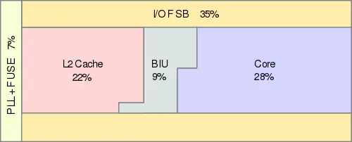
Bonnell has two address generation units (AGUs). For data, there is 24 KiB write-back L1 cache with a 2-level DTLB hierarchy, hardware page walker, and an integer store-to-load forwarding support. Additionally, there is a rather large 512 KiB L2 cache with inline ECC and hardware pre-fetchers. The tag, LRU, and the state bits are all stored in a single array to minimize area. The tag and data consist of 8 4.5 KiB tag sub arrays and 32 17.5 KiB data sub-arrays made of 256 cells on the bit line and 136 cells on the write line.
As a power-saving feature, the L2 cache can be configured down to 2-way dynamically. Additionally, for less demanding tasks, the Bonnell power gates unused ways. It's interesting to note that the design team placed the TAG blocks at the bottom of the DATA arrays allowing, in theory, to expend the L2 to 1 MiB should they want to.
I/O Bus
- Main article: Front-Side Bus
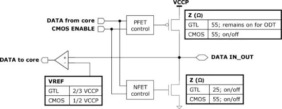
Traditionally, Intel has been using AGTL+ transceivers (Advanced Gunning Transceiver Logic) for their front-side bus communication. With bonnell (and the chipset) Intel also introduced a CMOS signaling logic mode. CMOS has the advantage of only drawing power during transition. The switch to CMOS saves 200-500 mW at the cost of worse latency and slower bus which ranges from 400 to 533 MHz. Bonnell's intended applications is not heavy processing machine, the lower bus speed was likely a worthy compromise.
Bonnell implements both mode, so designers who prefer the faster bus can opt for the traditional AGTL+ transceivers while those who seek low power can opt for the CMOS implementation. Intel offers both types by simply fusing the appropriate circuitry. This is done by reprogramming the NFET control pull-down and the PFET control accordingly.
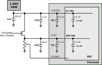
Note that during deep sleep, the design team designed the power rails using two power planes. To further save power, only keeping 21 pins are kept alive, reducing the average power by another 10% while killing off 182 of the other I/O which are not necessary for that state.
Features
Multithreading
Bonnell supports Intel's Hyper-Threading, their marketing term for their own implementation of simultaneous multithreading. The notion of implementing simultaneous multithreading on such a low-power architecture might seem unusual at first. In fact, it's one of only a handful of ultra-low power architectures to support such feature. Intel justified this design choice by demonstrating that performance enjoys an uplift of anywhere from 30% to 50% while worsening power consumption by up to 20% (with an average of 30% performance increase for 15% more power). The toll on the die area was a mere 8%.
In the front-end, the prefetch buffer and the instruction queue have been duplicated for each thread, everything else is competitively shared between the threads. In the back-end, only the integer and floating register files are duplicated, everything else is competitively shared as well. Note that both threads compete over the L1 instruction and data caches as well as the L2 and the TLBs with the exception of a 16-entry micro-TLB that's duplicated for each thread.
Low-power features
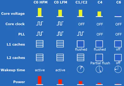
Bonnell implements a number of features to enhance battery life including several lower power states (C-states). Bonnell is capable of achieving 2 GHz core frequency at 1 V and can go down all the way to 600 MHz at 0.75 V though down-dialing the core phase-lock-loop (PLL) ratio. Bonnell supports up to C6 C-state where more power saving is achieving with higher C-state which in term means more components (i.e., features) are turned off.
• C-0 state, the processor can operate at its highest frequency (in high-frequency mode (HFM)) and in its lowest frequency (low frequency mode (LFM)).
• C-1 state, the core is power-gated and the L1 caches are flushed, yielding lower dynamic power; exit latency is sub-1µs
• C-4 state, the PPLs are shut down down as well, exit latency is in the order of 30 µs
• C-6 state, the state of the machine is kept alive in a 10.5 KiB register file (SRAM kept at VCC of 0.3 V) with the core power is completely shut off; exit latency in the order of 100 µs
Intel estimates C-6 residency to be between 80% and 90% resulting in an average power in the order of 220 mW. Likewise Idle power, which is dominated by leakage power of the functional units, is below 80 mW.
Die
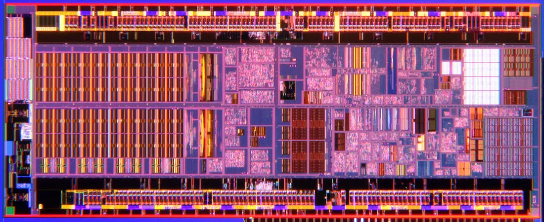
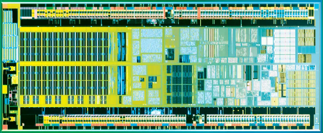
Silverthorne
- 45 nm process
- 9 metal layers
- 47,212,207 transistors
- 3.1 mm x 7.8 mm
- 24.2 mm² die size
- packaged in a Halide-Free 441 ball, 14 mm x 13 mm µFCBGA
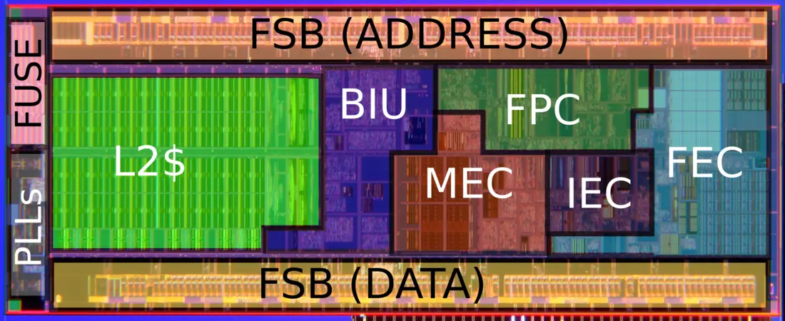
Function Unit Blocks (FUBs):
- BIC/BIU - Bus Interface Cluster/Unit
- MEC - Memory Cluster Execution & L1d$
- FPC - FP/SIMD execution Cluster
- IEC - Integer Execution Cluster
- FEC - Front-End Cluster & L1i$
- FSB - Front Side Bus
Physical layout
The Atom design team was considerably smaller than Intel's typical design teams which forced them to work in a slightly different way. The design team used a methodology they described as a "sea of Functional Unit Block" (FUBs) where by all cluster hierarchies (including unit-level hierarchies) are flattened at the chip level. This development methodology allowed for faster iteration. The various FUB designs were divided among the team members allowing them to handle the design in a more manageable way. All in all, Bonnell's physical database consisted of 205 unique FUBs interlinked via 41,000 FUB-to-FUB interconnects. Bonnell is manufactured on Intel's 45 nm process. 91% of the FUBs using pre-characterized standard cells (45% structured data-path and 46% fully synthesized random logic blocks) with only the remaining 9% being full-custom blocks. The unusually high utilization of standard cells (at least for Intel) is likely due to the limited resources given to the Bonnell design team.
| Type | Unique | Instances |
|---|---|---|
| Random Logic Synthesized | 92 | 92 |
| Structured Data Paths | 88 | 140 |
| L2 sub-arrays | 2 | 40 |
| Custom | 18 | 19 |
| Repeater Station | - | 317 |
| Total | 200 | 608 |
| Cluster | Transistor Count |
|---|---|
| Core | 13,828,574 |
| Uncore | 2,738,951 |
| L2 & L2 tag | 30,644,682 |
| Total | 47,212,207 |
Cores
First Generation
First generation of Bonnell-based microprocessors introduced 2 cores: Silverthorne for ultra-mobile PCs and mobile Internet devices (MIDs) and Diamondville for ultra cheap notebooks and desktops.
Silverthorne
- Main article: Silverthorne
Silverthorne was the codename for a series of Mobile Internet Devices (MIDs) introduced in 2008. These processors had 1 core and 2 threads with a FSB operating at 400 MHz-533 MHz.
Diamondville
- Main article: Diamondville
Diamondville was the codename for the series of ultra cheap notebooks and desktops introduced in 2008. Diamondville is very much a soldered-on-motherboard derivative of Silverthorne with faster FSB (operating at 533 MHz - 667 MHz). The dual-core version is an MCM (Multi Chip Module) Silverthorne variant.
Second Generation
First generation of Bonnell-based microprocessors while being low power had to work with the older 90 nm process 945GSE chipset and 82801GBM I/O controller with a TDP of almost 9.5 watts - almost 4 times that of the processor itself. Second generation Bonnell-based microprocessors aimed to address this issue by integrating a memory controller and GPU on-chip. This drastically reduced power consumption and cost.
Lincroft
- Main article: Lincroft
Lincroft is the codename for Bonnell-based Silverthorne's successor. Lincroft integrates on-die the graphics and memory controller.
Pineview
- Main article: Pineview
Pineview was the codename for second generate Bonnell-based processors which integrated a memory controller, Direct Media Interface (DMI) link, and the GMA 3150 GPU. Pineview is the successor for Diamondville, targeting the same ultra cheap desktops, nettops and netbooks.
Tunnel Creek
- Main article: Tunnel Creek
Tunnel Creek was the codename for a series of MPUs for embedded applications.
Stellarton
- Main article: Stellarton
Stellarton was the codename for a series of MPUs for embedded applications. Stellarton is the Tunnel Creek core packaged with an Altera FPGA.
Sodaville
- Main article: Sodaville
Sodaville is the codename for a series of consumer electronics system on a chip (e.g. set-top box).
Groveland
- Main article: Groveland
Groveland is the codename for a series of consumer electronics MPUs (e.g. smart TVs).
All Bonnell Chips
| Bonnell Chips | ||||||||||
|---|---|---|---|---|---|---|---|---|---|---|
| CPU | IGP | |||||||||
| Model | µarch | Platform | Core | Launched | SDP | Freq | Max Mem | Name | Freq | Max Freq |
| 230 | Bonnell | Nettop 2008 | Diamondville | 3 June 2008 | 1,599.99 MHz 1.6 GHz 1,599,990 kHz | 8,192 MiB 8,388,608 KiB 8,589,934,592 B 8 GiB 0.00781 TiB | ||||
| 330 | Bonnell | Nettop 2008 | Diamondville | 21 September 2008 | 1,599.99 MHz 1.6 GHz 1,599,990 kHz | 8,192 MiB 8,388,608 KiB 8,589,934,592 B 8 GiB 0.00781 TiB | ||||
| N270 | Bonnell | Nettop 2008 | Diamondville | 3 June 2008 | 1,599.99 MHz 1.6 GHz 1,599,990 kHz | 8,192 MiB 8,388,608 KiB 8,589,934,592 B 8 GiB 0.00781 TiB | ||||
| N280 | Bonnell | Nettop 2008 | Diamondville | 7 February 2009 | 1,666.66 MHz 1.667 GHz 1,666,660 kHz | 8,192 MiB 8,388,608 KiB 8,589,934,592 B 8 GiB 0.00781 TiB | ||||
| Z500 | Bonnell | Menlow | Silverthorne | 2 April 2008 | 0.96 W 960 mW 0.00129 hp 9.6e-4 kW | 800 MHz 0.8 GHz 800,000 kHz | ||||
| Z510 | Bonnell | Menlow | Silverthorne | 2 April 2008 | 0.96 W 960 mW 0.00129 hp 9.6e-4 kW | 1,100 MHz 1.1 GHz 1,100,000 kHz | ||||
| Z510P | Bonnell | Menlow | Silverthorne | 2 March 2009 | 1,100 MHz 1.1 GHz 1,100,000 kHz | |||||
| Z510PT | Bonnell | Menlow | Silverthorne | 2 March 2009 | 1,100 MHz 1.1 GHz 1,100,000 kHz | |||||
| Z515 | Bonnell | Menlow | Silverthorne | 8 April 2009 | 1,200 MHz 1.2 GHz 1,200,000 kHz | |||||
| Z520 | Bonnell | Menlow | Silverthorne | 2 April 2008 | 0.96 W 960 mW 0.00129 hp 9.6e-4 kW | 1,333.33 MHz 1.333 GHz 1,333,330 kHz | ||||
| Z520PT | Bonnell | Menlow | Silverthorne | 2 March 2009 | 1,333.33 MHz 1.333 GHz 1,333,330 kHz | |||||
| Z530 | Bonnell | Menlow | Silverthorne | 2 April 2008 | 1,599.99 MHz 1.6 GHz 1,599,990 kHz | |||||
| Z530P | Bonnell | Menlow | Silverthorne | 2 March 2009 | 1,599.99 MHz 1.6 GHz 1,599,990 kHz | |||||
| Z540 | Bonnell | Menlow | Silverthorne | 2 April 2008 | 0.96 W 960 mW 0.00129 hp 9.6e-4 kW | 1,866.66 MHz 1.867 GHz 1,866,660 kHz | ||||
| Z550 | Bonnell | Menlow | Silverthorne | 8 April 2009 | 1,999.99 MHz 2 GHz 1,999,990 kHz | |||||
| Z560 | Bonnell | Menlow | Silverthorne | June 2010 | 2,133.33 MHz 2.133 GHz 2,133,330 kHz | |||||
| Z600 | Bonnell | Moorestown | Lincroft | 4 May 2010 | 800 MHz 0.8 GHz 800,000 kHz | 1,024 MiB 1,048,576 KiB 1,073,741,824 B 1 GiB 9.765625e-4 TiB | PowerVR SGX535 | 200 MHz 0.2 GHz 200,000 KHz | ||
| Z605 | Bonnell | Moorestown | Lincroft | 4 May 2010 | 1,000 MHz 1 GHz 1,000,000 kHz | 2,048 MiB 2,097,152 KiB 2,147,483,648 B 2 GiB 0.00195 TiB | PowerVR SGX535 | 400 MHz 0.4 GHz 400,000 KHz | ||
| Z610 | Bonnell | Moorestown | Lincroft | 4 May 2010 | 800 MHz 0.8 GHz 800,000 kHz | 2,048 MiB 2,097,152 KiB 2,147,483,648 B 2 GiB 0.00195 TiB | PowerVR SGX535 | 400 MHz 0.4 GHz 400,000 KHz | ||
| Z612 | Bonnell | Moorestown | Lincroft | 4 May 2010 | 900 MHz 0.9 GHz 900,000 kHz | 2,048 MiB 2,097,152 KiB 2,147,483,648 B 2 GiB 0.00195 TiB | PowerVR SGX535 | 400 MHz 0.4 GHz 400,000 KHz | ||
| Z615 | Bonnell | Moorestown | Lincroft | 4 May 2010 | 1,200 MHz 1.2 GHz 1,200,000 kHz | 2,048 MiB 2,097,152 KiB 2,147,483,648 B 2 GiB 0.00195 TiB | PowerVR SGX535 | 400 MHz 0.4 GHz 400,000 KHz | ||
| Z620 | Bonnell | Moorestown | Lincroft | 4 May 2010 | 900 MHz 0.9 GHz 900,000 kHz | 2,048 MiB 2,097,152 KiB 2,147,483,648 B 2 GiB 0.00195 TiB | PowerVR SGX535 | 400 MHz 0.4 GHz 400,000 KHz | ||
| Z625 | Bonnell | Moorestown | Lincroft | 4 May 2010 | 1,500 MHz 1.5 GHz 1,500,000 kHz | 2,048 MiB 2,097,152 KiB 2,147,483,648 B 2 GiB 0.00195 TiB | PowerVR SGX535 | 400 MHz 0.4 GHz 400,000 KHz | ||
| Z650 | Bonnell | Oak Trail | Lincroft | 11 April 2011 | 1,200 MHz 1.2 GHz 1,200,000 kHz | 2,048 MiB 2,097,152 KiB 2,147,483,648 B 2 GiB 0.00195 TiB | PowerVR SGX535 | 400 MHz 0.4 GHz 400,000 KHz | ||
| Z670 | Bonnell | Oak Trail | Lincroft | 11 April 2011 | 1,500 MHz 1.5 GHz 1,500,000 kHz | 2,048 MiB 2,097,152 KiB 2,147,483,648 B 2 GiB 0.00195 TiB | PowerVR SGX535 | 400 MHz 0.4 GHz 400,000 KHz | ||
References
- Some information was obtained directly from Intel
- Gerosa, Gianfranco, et al. "A sub-2 W low power IA processor for mobile internet devices in 45 nm high-k metal gate CMOS." IEEE Journal of Solid-State Circuits 44.1 (2009): 73-82.
- Gerosa, Gianfranco, et al. "A sub-1W to 2W low-power IA processor for mobile internet devices and ultra-mobile PCs in 45nm hi-κ metal gate CMOS." Solid-State Circuits Conference, 2008. ISSCC 2008. Digest of Technical Papers. IEEE International. IEEE, 2008.
- Taufique, Mohammed H., et al. "A 512-KB level-2 cache design in 45-nm for low power IA processor silverthorne." Custom Integrated Circuits Conference, 2008. CICC 2008. IEEE. IEEE, 2008.
- Wang, Perry H., et al. "Intel® atom™ processor core made FPGA-synthesizable." Proceedings of the ACM/SIGDA international symposium on Field programmable gate arrays. ACM, 2009.
| codename | Bonnell + |
| core count | 1 + and 2 + |
| designer | Intel + |
| first launched | March 2, 2008 + |
| full page name | intel/microarchitectures/bonnell + |
| instance of | microarchitecture + |
| instruction set architecture | IA-32 + and x86-64 + |
| manufacturer | Intel + |
| microarchitecture type | CPU + |
| name | Bonnell + |
| phase-out | 2011 + |
| pipeline stages (max) | 19 + |
| pipeline stages (min) | 16 + |
| process | 45 nm (0.045 μm, 4.5e-5 mm) + |
