| Line 13: | Line 13: | ||
| pipeline = Yes | | pipeline = Yes | ||
| type = Superscalar | | type = Superscalar | ||
| − | |||
| OoOE = No | | OoOE = No | ||
| speculative = No | | speculative = No | ||
Revision as of 02:50, 23 March 2017
| Edit Values | |
| Bonnell µarch | |
| General Info | |
| Arch Type | CPU |
| Designer | Intel |
| Manufacturer | Intel |
| Introduction | 2008 |
| Phase-out | 2011 |
| Process | 45 nm |
| Core Configs | 1, 2 |
| Pipeline | |
| Type | Superscalar |
| Speculative | No |
| Reg Renaming | No |
| Stages | 16 |
| Instructions | |
| ISA | IA-32, x86-64 |
| Extensions | MOVBE, MMX, SSE, SSE2, SSE3, SSSE3 |
| Cache | |
| L1I Cache | 32 KiB/Core 8-way set associative |
| L1D Cache | 24 KiB/Core 6-way set associative |
| L2 Cache | 512 KiB/Core 8-way set associative |
| Cores | |
| Core Names | Silverthorne, Diamondville, Lincroft, Pineview, Tunnel Creek, Stellarton, Sodaville, Groveland |
| Succession | |
Bonnell was a microarchitecture for Intel's 45 nm ultra-low power microprocessors first introduced in 2008 for their then-new Atom family. Bonnell, which was named after the highest point in Austin - Mount Bonnell, was Intel's first x86-compatible microarchitecture designed to target the ultra-low power market.
Bonnell (project Silverthorne then) was designed by a then-new low-power design team Intel created at their Texas Development Center in Austin in 2004 along with a new chipset (Poulsbo) design team. The design team was led by Elinora Yoeli. While Yoeli previously worked at her native country, Bonnell was a US design and was unconnected to any of Intel's projects worked on by the Israel Design Center in Haifa. Previously Yoeli led the Israeli team in the development of Pentium M.
Contents
Codenames
| Chipset | Platform | PHC | Core | Target |
|---|---|---|---|---|
| Poulsbo | Menlow | Silverthorne | MIDs | |
| Poulsbo | Menlow | Diamondville | Nettops | |
| Moorestown | Langwell | Lincroft | MIDs | |
| Pine Trail | Tiger Point | Pineview | Nettops | |
| Queens Bay | Topcliff | Tunnel Creek | Embedded | |
| Queens Bay | Topcliff | Stellarton | Embedded + Altera FPGA | |
| Sodaville | CE | |||
| Groveland | CE |
Generation successor
| First Generation | Second Generation | |
|---|---|---|
| Silverthorne | → | Lincroft |
| Diamondville | → | Pineview |
| Tunnel Creek | ||
| Stellarton | ||
| Sodaville | ||
| Groveland |
Release Dates
Bonnell was first announced on April 2nd 2008 during the Intel Developers Forum in Shanghai.
Process Technology
| 45 nm Manufacturing Fabs | |
|---|---|
| Fab | Location |
| D1D | Hillsboro, Oregon |
| Fab 32 | Chandler, Arizona |
| Fab 28 | Kiryat Gat, Israel |
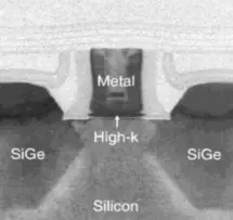
Bonell is designed to be manufactured using a 45 nm process. Intel's 45 nm process is the first high-volume manufacturing process to introduce High-k + metal gate transistors.
| Bonnell | |
|---|---|
| 45 nm | |
| Gate Pitch | 180 nm |
| Interconnect Pitch | 160 nm |
| SRAM bit cell (HD) | 0.346 µm² |
| SRAM bit cell (LP) | 0.382 µm² |
Compiler support
| Compiler | Arch-Specific | Arch-Favorable |
|---|---|---|
| GCC | -march=bonnell |
-mtune=bonnell
|
| LLVM | -march=bonnell |
-mtune=bonnell
|
| Visual Studio | /arch:SSE3
|
Architecture
Bonnell features a brand new architecture not based on any previous Intel design. The architecture was specifically designed for ultra-mobile PCs (UMPCs), mobile internet devices (MID), and other embedded devices. Bonnell's primary goals were:
- Reduce power consumption,
- while staying fully x86-compatible,
- at acceptable performance
Performance/Power new rule: +1% performance for at most +1% power consumption.
Architecture
- Strictly ultra-low power
- 45 nm process, 9 metal layers, CMOS
- 500 mW to 2 W TDP
- 533 MT/s dual mode (GTL & CMOS) FSB
- In-order
- 2-issue decode
- Simple 2-way SMT
- Instruction Queue of 16 entries/thread
- FP Register File (per thread)
- Integer Register File (per thread)
- Private L1 cache for each core
- Shared L2 cache for the entire chip
The number of functional units were kept to minimum to cut on power consumption.
- 2 address generation units (AGUs)
- 2 Integer ALUs (1 for jumps, 1 for shifts)
- 2 FP ALUs (1 adder, 1 for others)
- No Integer multiplier & divider (shared with FP ALU instead)
Memory Hierarchy
- Cache
- Hardware prefetchers
- C6 cache
- 10.5 KiB array to hold the architectural state during deep power down state
- L1 Data Cache
- 32 KiB
- 8-way set associative
- 1 read and 1 write port
- 8 transistors (instead of 6) to reduce voltage
- L1 Instruction Cache
- 24 KiB
- 6-way set associative
- 1 read and 1 write port
- 8 transistors (instead of 6) to reduce voltage
- Per core
- L2 Cache:
- 512 KiB 8-way set associative
- ECC
- Shrinkable from 512 KiB to 128 KiB (2-way)
- Per core
- L3 Cache:
- No level 3 cache
- RAM
- Maximum of 2 GiB, 4 GiB, and 8 GiB
Note that the L1 cache for data and instructions were originally both 32 KiB (8-way), however due to power restrictions, the L1d$ was later reduced to 24 KiB.
Pipeline
Bonnell's architecture shares very little in common with other Intel designs. To achieve the strict ultra-low power objects, Bonnell features a very slimmed own design discarding many high-performance techniques used by Intel's high-performance architectures such as aggressive speculative execution, out-of-order execution, and µop transformation.
Bonnell consists of an in-order dual-issue 16-stage pipeline. Bonnell supports 2-way SMT
The longer pipeline allows a more evenly spreading of heat across the chip with more units. This also allows a higher clock rate.
- Instruction Fetch
- 3 stages
- 8 Bytes/Cycle (lower if SMT)
- Instruction Decode
- 3 stages
- Instructions with up to 3 prefixes/Cycle
- Instruction Dispatch
- 2 stages
- Source Operand Read
- 1 stage
- reading register operand
- 1 stage
- Data Cache Access
- 3 stages
- 1 stage for calculating
- 2 stages for reading cache
- 3 stages
- Execution
- 2 clusters
- integers
- quick cache access due to direct connection
- floating point & SIMD
- integers
- 2 clusters
- Exception & MT Handling
- 2 stages
- Commit
- 1 stage
Multithreading
Bonnell has support for multithreading - up to two threads per core. However each thread compete for the same resources which does inherently means they run slower than they would if they were to run alone.
Branch Prediction
- Two-level adaptive predictor
- 12-bit branch history register
- Pattern history table has 4096 entries (shared between threads)
- Branch buffer target has 128 entries (4-way, 32 sets)
- Unconditional jumps are ignored
- Always-taken and never-taken are marked in the table
- Penalties:
- 13 stages for miss prediction
- 7 stages for correct prediction but missing branch target buffer (BTB)
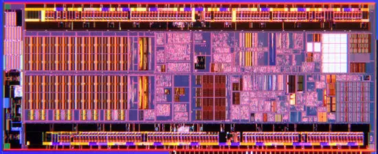
Die
- 45 nm process
- 9 metal layers
- 47,000,000 transistors
- 3.1 mm x 7.8 mm
- 24.2 mm² die size
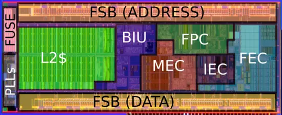
- BIC - Bus Interface Cluster
- MEC - Memory Cluster Execution & L1d$
- FPC - FP/SIMD execution Cluster
- IEC - Integer Execution Cluster
- FEC - Front-End Cluster & L1i$
- FSB - Front Side Bus
Cores
First Generation
First generation of Bonnell-based microprocessors introduced 2 cores: Silverthorne for ultra-mobile PCs and mobile Internet devices (MIDs) and Diamondville for ultra cheap notebooks and desktops.
Silverthorne
- Main article: Silverthorne
Silverthorne was the codename for a series of Mobile Internet Devices (MIDs) introduced in 2008. These processors had 1 core and 2 threads with a FSB operating at 400 MHz-533 MHz.
Diamondville
- Main article: Diamondville
Diamondville was the codename for the series of ultra cheap notebooks and desktops introduced in 2008. Diamondville is very much a soldered-on-motherboard derivative of Silverthorne with faster FSB (operating at 533 MHz - 667 MHz). The dual-core version is an MCM (Multi Chip Module) Silverthorne variant.
Second Generation
First generation of Bonnell-based microprocessors while being low power had to work with the older 90 nm process 945GSE chipset and 82801GBM I/O controller with a TDP of almost 9.5 watts - almost 4 times that of the processor itself. Second generation Bonnell-based microprocessors aimed to address this issue by integrating a memory controller and GPU on-chip. This drastically reduced power consumption and cost.
Lincroft
- Main article: Lincroft
Lincroft is the codename for Bonnell-based Silverthorne's successor. Lincroft integrates on-die the graphics and memory controller.
Pineview
- Main article: Pineview
Pineview was the codename for second generate Bonnell-based processors which integrated a memory controller, Direct Media Interface (DMI) link, and the GMA 3150 GPU. Pineview is the successor for Diamondville, targeting the same ultra cheap desktops, nettops and netbooks.
Tunnel Creek
- Main article: Tunnel Creek
Tunnel Creek was the codename for a series of MPUs for embedded applications.
Stellarton
- Main article: Stellarton
Stellarton was the codename for a series of MPUs for embedded applications. Stellarton is the Tunnel Creek core packaged with an Altera FPGA.
Sodaville
- Main article: Sodaville
Sodaville is the codename for a series of consumer electronics system on a chip (e.g. set-top box).
Groveland
- Main article: Groveland
Groveland is the codename for a series of consumer electronics MPUs (e.g. smart TVs).
All Bonnell Chips
| Bonnell Chips | ||||||||||
|---|---|---|---|---|---|---|---|---|---|---|
| CPU | IGP | |||||||||
| Model | µarch | Platform | Core | Launched | SDP | Freq | Max Mem | Name | Freq | Max Freq |
| 230 | Bonnell | Nettop 2008 | Diamondville | 3 June 2008 | 1,599.99 MHz 1.6 GHz 1,599,990 kHz | 8,192 MiB 8,388,608 KiB 8,589,934,592 B 8 GiB 0.00781 TiB | ||||
| 330 | Bonnell | Nettop 2008 | Diamondville | 21 September 2008 | 1,599.99 MHz 1.6 GHz 1,599,990 kHz | 8,192 MiB 8,388,608 KiB 8,589,934,592 B 8 GiB 0.00781 TiB | ||||
| N270 | Bonnell | Nettop 2008 | Diamondville | 3 June 2008 | 1,599.99 MHz 1.6 GHz 1,599,990 kHz | 8,192 MiB 8,388,608 KiB 8,589,934,592 B 8 GiB 0.00781 TiB | ||||
| N280 | Bonnell | Nettop 2008 | Diamondville | 7 February 2009 | 1,666.66 MHz 1.667 GHz 1,666,660 kHz | 8,192 MiB 8,388,608 KiB 8,589,934,592 B 8 GiB 0.00781 TiB | ||||
| Z500 | Bonnell | Menlow | Silverthorne | 2 April 2008 | 0.96 W 960 mW 0.00129 hp 9.6e-4 kW | 800 MHz 0.8 GHz 800,000 kHz | ||||
| Z510 | Bonnell | Menlow | Silverthorne | 2 April 2008 | 0.96 W 960 mW 0.00129 hp 9.6e-4 kW | 1,100 MHz 1.1 GHz 1,100,000 kHz | ||||
| Z510P | Bonnell | Menlow | Silverthorne | 2 March 2009 | 1,100 MHz 1.1 GHz 1,100,000 kHz | |||||
| Z510PT | Bonnell | Menlow | Silverthorne | 2 March 2009 | 1,100 MHz 1.1 GHz 1,100,000 kHz | |||||
| Z515 | Bonnell | Menlow | Silverthorne | 8 April 2009 | 1,200 MHz 1.2 GHz 1,200,000 kHz | |||||
| Z520 | Bonnell | Menlow | Silverthorne | 2 April 2008 | 0.96 W 960 mW 0.00129 hp 9.6e-4 kW | 1,333.33 MHz 1.333 GHz 1,333,330 kHz | ||||
| Z520PT | Bonnell | Menlow | Silverthorne | 2 March 2009 | 1,333.33 MHz 1.333 GHz 1,333,330 kHz | |||||
| Z530 | Bonnell | Menlow | Silverthorne | 2 April 2008 | 1,599.99 MHz 1.6 GHz 1,599,990 kHz | |||||
| Z530P | Bonnell | Menlow | Silverthorne | 2 March 2009 | 1,599.99 MHz 1.6 GHz 1,599,990 kHz | |||||
| Z540 | Bonnell | Menlow | Silverthorne | 2 April 2008 | 0.96 W 960 mW 0.00129 hp 9.6e-4 kW | 1,866.66 MHz 1.867 GHz 1,866,660 kHz | ||||
| Z550 | Bonnell | Menlow | Silverthorne | 8 April 2009 | 1,999.99 MHz 2 GHz 1,999,990 kHz | |||||
| Z560 | Bonnell | Menlow | Silverthorne | June 2010 | 2,133.33 MHz 2.133 GHz 2,133,330 kHz | |||||
| Z600 | Bonnell | Moorestown | Lincroft | 4 May 2010 | 800 MHz 0.8 GHz 800,000 kHz | 1,024 MiB 1,048,576 KiB 1,073,741,824 B 1 GiB 9.765625e-4 TiB | PowerVR SGX535 | 200 MHz 0.2 GHz 200,000 KHz | ||
| Z605 | Bonnell | Moorestown | Lincroft | 4 May 2010 | 1,000 MHz 1 GHz 1,000,000 kHz | 2,048 MiB 2,097,152 KiB 2,147,483,648 B 2 GiB 0.00195 TiB | PowerVR SGX535 | 400 MHz 0.4 GHz 400,000 KHz | ||
| Z610 | Bonnell | Moorestown | Lincroft | 4 May 2010 | 800 MHz 0.8 GHz 800,000 kHz | 2,048 MiB 2,097,152 KiB 2,147,483,648 B 2 GiB 0.00195 TiB | PowerVR SGX535 | 400 MHz 0.4 GHz 400,000 KHz | ||
| Z612 | Bonnell | Moorestown | Lincroft | 4 May 2010 | 900 MHz 0.9 GHz 900,000 kHz | 2,048 MiB 2,097,152 KiB 2,147,483,648 B 2 GiB 0.00195 TiB | PowerVR SGX535 | 400 MHz 0.4 GHz 400,000 KHz | ||
| Z615 | Bonnell | Moorestown | Lincroft | 4 May 2010 | 1,200 MHz 1.2 GHz 1,200,000 kHz | 2,048 MiB 2,097,152 KiB 2,147,483,648 B 2 GiB 0.00195 TiB | PowerVR SGX535 | 400 MHz 0.4 GHz 400,000 KHz | ||
| Z620 | Bonnell | Moorestown | Lincroft | 4 May 2010 | 900 MHz 0.9 GHz 900,000 kHz | 2,048 MiB 2,097,152 KiB 2,147,483,648 B 2 GiB 0.00195 TiB | PowerVR SGX535 | 400 MHz 0.4 GHz 400,000 KHz | ||
| Z625 | Bonnell | Moorestown | Lincroft | 4 May 2010 | 1,500 MHz 1.5 GHz 1,500,000 kHz | 2,048 MiB 2,097,152 KiB 2,147,483,648 B 2 GiB 0.00195 TiB | PowerVR SGX535 | 400 MHz 0.4 GHz 400,000 KHz | ||
| Z650 | Bonnell | Oak Trail | Lincroft | 11 April 2011 | 1,200 MHz 1.2 GHz 1,200,000 kHz | 2,048 MiB 2,097,152 KiB 2,147,483,648 B 2 GiB 0.00195 TiB | PowerVR SGX535 | 400 MHz 0.4 GHz 400,000 KHz | ||
| Z670 | Bonnell | Oak Trail | Lincroft | 11 April 2011 | 1,500 MHz 1.5 GHz 1,500,000 kHz | 2,048 MiB 2,097,152 KiB 2,147,483,648 B 2 GiB 0.00195 TiB | PowerVR SGX535 | 400 MHz 0.4 GHz 400,000 KHz | ||
| codename | Bonnell + |
| core count | 1 + and 2 + |
| designer | Intel + |
| first launched | 2008 + |
| full page name | intel/microarchitectures/bonnell + |
| instance of | microarchitecture + |
| instruction set architecture | IA-32 + and x86-64 + |
| manufacturer | Intel + |
| microarchitecture type | CPU + |
| name | Bonnell + |
| phase-out | 2011 + |
| pipeline stages | 16 + |
| process | 45 nm (0.045 μm, 4.5e-5 mm) + |


