| Edit Values | |
| SX-Aurora µarch | |
| General Info | |
| Arch Type | VPU |
| Designer | NEC |
| Manufacturer | TSMC |
| Introduction | 2018 |
| Core Configs | 8 |
| Pipeline | |
| Type | Superscalar, Pipelined |
| OoOE | Yes |
| Speculative | Yes |
| Reg Renaming | Yes |
| Stages | 8 |
| Decode | 4-way |
| Cache | |
| L1I Cache | 32 KiB/core |
| L1D Cache | 32 KiB/core |
| L2 Cache | 256 KiB/core |
| L3 Cache | 16 MiB/chip |
| Succession | |
SX-Aurora is the successor to the SX-ACE, a 16 nm vector processor microarchitecture designed by NEC and introduced in 2018.
Contents
History[edit]
The SX-Aurora is the successor to the SX-ACE, a series of vector processors that NEC has been developing since the early 1980s. NEC first announced the SX-Aurora TSUBASA product line on October 26 2017 with a complete lineup that ranges from a workstation featuring one vector engine (VE) card to a full supercomputer with 64 VEs. NEC disclosed the architecture of the chip at Hot Chips 30 in August 2018.
Architecture[edit]
Key changes from SX-ACE[edit]
- Accelerator architecture (From self-hosted)
- Relies on an x86 host
- 16 nm process (from 28 nm)
- 1.6x frequency (1.6 GHz, up from 1 GHz)
- 2x vector cores (8, up from 4)
- Vector core
- 1.5x FMAs EUs (3, up from 2)
- 2x VPPs (32, up from 16)
- 3x FLOPs/cycle (192 FLOPs/cycle, up from 64 FLOPs/cycle)
- Memory
This list is incomplete; you can help by expanding it.
Block Diagram[edit]
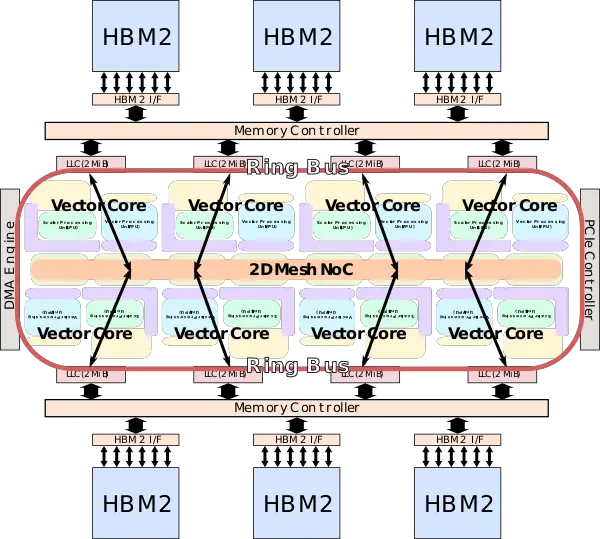
Entire SoC[edit]
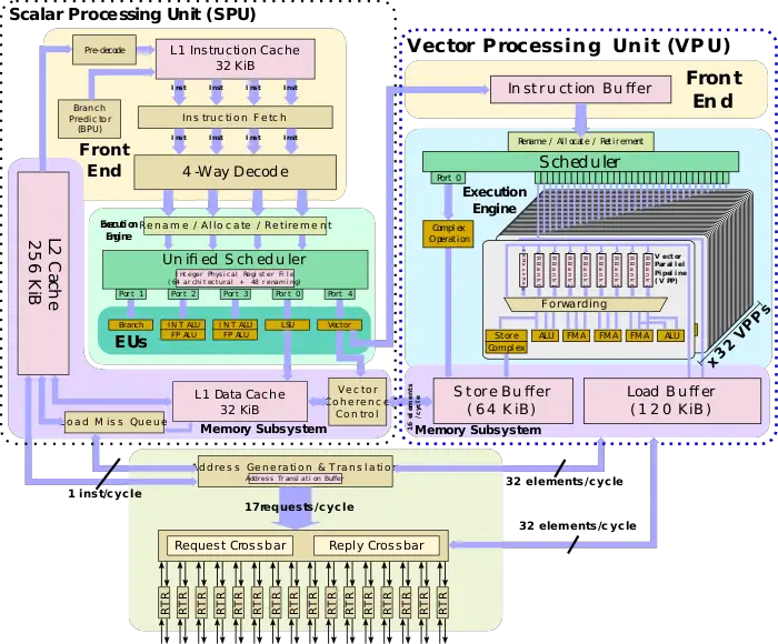
Vector core[edit]
Memory Hierarchy[edit]
- Vector core
- SPU
- L1I Cache:
- 32 KiB
- L1D Cache:
- 32 KiB
- L2 Cache:
- 256 KiB
- L1I Cache:
- VPU
- 120 KiB load buffer
- 64 KiB store buffer
- SPU
- L3 Cache/LLC:
- 16 MiB
- 8 x 2 MiB
- write-back
- inclusive of L1 & L2
- 128 banks
- 3 TiB/s bandwidth
- 16 MiB
- System DRAM:
Overview[edit]
The SX-Aurora is NEC's successor to the SX-ACE, a vector processor designed for high-performance scientific/research applications and supercomputers. The SX-Aurora deviates from all prior chips in the kind of markets it's designed to address. Therefore, NEC made slightly different design choice compared to prior generations of vector processors. In an attempt to broaden their market, NEC extended beyond supercomputers to the conventional server and workstation market. This is done through the use of PCIe-based accelerator cards.
Moving to an accelerator card is not without its challenges. To keep the high memory bandwidth, and thus high bytes per FLOP, while moving a smaller form factor, it was necessary to drop the large amount of DDR memory channels. Instead, NEC opted to utilizing high-bandwidth memory on-chip instead. The card itself is designed to communicate with other cards on the system in order to scale up from just a single card for workstation use to a supercomputer with 64 cards per rack.
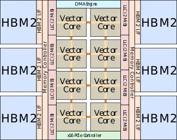
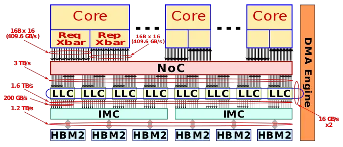
The chip itself consists of eight very big cores along with 16 MiB of last level cache on a 2-dimensional mesh. Attached to the LLC are the two memory controllers which interface with the six high-bandwidth memory sitting on an interposer. Fabricated on TSMC's 16 nm process, the SX-Aurora operates at up to 1.6 GHz delivering up to 307.2 gigaFLOPS (double-precision) per core for a total of up to 2.45 teraFLOPS.
Vector core[edit]
Like its predecessor, the SX-Aurora vector core itself has three main components - the scalar processing unit (SPU), the vector processing unit (VPU), and the memory subsystem. Though all three were enhanced over the SX-ACE, the emphasis was on the VPU and the new memory subsystem. The majority of the compute capability is in the VPU which can deliver up to 192 DP FLOPS per cycle for up to 307.2 GFLOPS at 1.6 GHz. The VPU is fed by a high-bandwidth mesh capable of 256 B/cycle for a total of up to 410 GB/s for load and store each. The SPU is designed to provide all basic functionalities a typical CPU. Because the SX-Aurora is not a typical offload engine but a self-hosted accelerator, the SPU is designed to deliver high performance to keep pace with the VPU and other operating system-related tasks.
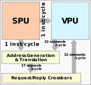
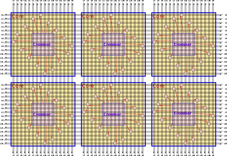
The memory subsystem on the SX-Aurora has been greatly enhanced from the SX-ACE. The primary focus of here is to support contiguous vector memory accesses. To that end, in order to feed the vector pipeline, the address generation unit can receive a vector instruction from the SPU in advance in order to calculate the address and disperse the request to the sixteen ports on the mesh network. 16 elements/cycle vector address generation and translation, as well as 17 requests issued/cycle, can be performed. The bandwidth of the crossbars is matched with the bandwidth of the loads and stores at 256 B/cycle for up to 410 GB/s for load and stores each.
Scalar processing unit[edit]
Although the majority of the processing is handled by the VPU, the scalar processing unit (SPU) has to have a reasonably high performance in order to act as a host CPU for all the serial workloads including handling all the required operating system tasks. Additionally, the SPU has to provide the VPU with a sufficient stream of operations in order to maintain a high sustained performance as well as to calculate the base memory address for vector accesses.
Front-end[edit]
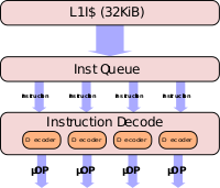
The SPU has 32 KiB of level 1 cache from which it fetches instructions from. The SPU on the SX-Aurora is four wide - capable of fetching and decoding four instructions per cycle. NEC stated that the SPU features a sophisticated branch predictor for hardware prefetching, however, they did not delve into any details. The SPU supports out-of-order execution with 8 stages of speculative execution.
Back end[edit]
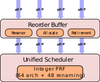
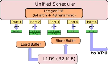
On the back end, the SPU includes a unified scheduler capable of issuing up to five instructions per cycle. Instructions are issued out-of-order once dependencies are resolved. The SX-Aurora has five separate execution units - two general ALUs for both integer and floating-point pipelines for general scalar arithmetic, a dedicated branch ALU, a single LSU execution unit, and a vector EU. Beyond the typical scalar operations, the SPU is required to calculate the base memory address for the vector accesses. Typically this is done prior to the vector instructions being sent to the VPU in order to ensure that the data is ready by that time. The SPU features a vector coherence control logic which supports high-speed vector memory accesses with up to 16 elements/cycle for vector stores. The SPU can send up to a single instruction to the VPU each cycle which goes to the instruction buffer of the VPU for reodering and scheduling.
Vector processing unit[edit]
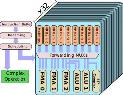
The bulk of the compute work is done on the vector processing unit (VPU). The VPU has a fairly simple pipeline, though it does employ out-of-order scheduling. Instructions issued by the SPU are sent to the instruction buffer where they await renaming, reordering, and scheduling. NEC renames the 64 architectural vector registers (VRs) onto 256 physical registers. There is support for enhanced preloading and avoids WAR/WAW dependencies. Scheduling is relatively simple. There is a dedicated pipeline for complex operations. Things such as vector summation, division, mask population count, are sent to this execution unit. The dedicate execution unit for complex operations is there to prevent stalls due to the high latency involved in those operations.
The majority of the operations are handled by the vector parallel pipeline (VPP). The SX-Aurora doubles the number of VPPs per VPU from the SX-ACE. Each VPU now has 32 VPPs - all identical. Note that all of the control logic described before are outside of the VPP which is relatively a simple block of vector execution. The VPP has an eight-port vector register, 16 mask registers, and six execution pipes, and a set of forwarding logic between them.
The six execution pipes include three floating-point pipes, two integer ALUs, and a complex and store pipe for data output. Note that ALU1 and the Store pipe share the same read ports. Likewise, FMA2 and ALU0 share a read port. All in all, the effective number of pipelines executing each cycle is actually four. Compared to the SX-Ace, the SX-Aurora now has one extra FMA unit per VPP. The VPP is designed such that all three FMAs can execute each cycle – each one can be independently operated by a different vector instruction. Every FMA unit is 64-bit wide and can support narrower packed operation such as 32-bit for double the peak theoretical performance. NEC's SX architecture has a very wide vector length the size of 256 elements with each element being 8 bytes (i.e., 2 KiB). Therefore a single vector operation requires eight cycles to complete by a single FMA pipeline across all 32 VPPS.
The peak theoretical performance that can be achieved is 3 FMAs per VPP per cycle. With 32 VPPs per VPU, there are a total of 96 FMAs/cycle for a total of 192 DP FLOPs/cycle. With a peak frequency of 1.6 GHz for the SX-Aurora Tsubasa vector processor, each VPU has a peak performance of 307.2 gigaFLOPS. Each FMA can perform operations on packed data types. That is, the single-precision floating-point is doubled through the packing of 2 32-bit elements for a peak performance of 614.4 gigaFLOPS.
Memory subsystem[edit]
Maintaining a high bytes Per FLOP is important for vector operations that rely on large data sets. With over five times the FLOPS per core, the SX-Aurora had to significantly improve the memory subsystem to prevent workloads from memory bottlenecking, thereby preventing them from reaching the peak compute power of the chip. The SX-Ace reached 256 GB/s of memory bandwidth using a whopping 16 channels of DDR3 memory. It becomes impossible to increase this further to bring a sufficiently large improvement in bandwidth. For this reason, NEC opted to use HBM2 memory instead. The SX-Aurora has six HBM2 modules delivering 1.22 TB/s of bandwidth, nearly 5-fold improvement over the SX-Ace. However, despite the large memory bandwidth improvement, the SX-Aurora achieves 0.5 bytes/FLOPs which is half of the SX-Ace.
The SX-Aurora got rid of the 1 MiB assignable data buffer (ADB) from the SX-Ace and added a memory side cache designed to avoid snoop traffic. It's worth pointing out that the new LLC does retain an ADB-like feature whereby the priority of a cache line is controlled via a flag for vector memory access instructions. The caches are sliced into eight 2 MiB chunks which consist of 16 memory banks each for a total of 128 memory banks. The LLC is inclusive of both the L1 and L2. The LLC interfaces with the IMC at 200 GB/s per chunk (1600 TB/s in total) and those provide a memory bandwidth of 1.22 TB/s through it's 6 HBM2 modules.
B/FLOP[edit]
- Main article: Bytes Per FLOP (B/F)
| Type | HBM:SoC | LLC:NoC | NoC:Core |
|---|---|---|---|
| Rate | 0.5 B/FLOP | 1.22 B/FLOP | 2.67 B/FLOP |
Mesh interconnect[edit]
All eight cores are interconnected using a 2D mesh network. The designed favored minimal wiring for maximum bandwidth. The SX-Aurora features a 16-layer 2D mesh network that uses dimension-ordered routing along with virtual channels for requests and replies. As illustrated in the diagram below, the router crossbar points are arranged in a diamond shape in order to minimize distance to the request and reply crossbars in the core. With the SX-Ace, replies to the cores were slightly unbalanced. In the SX-Aurora, the requests crossbars and the reply crossbars, each, have the same bandwidth. With each request being 16B, this works out to around 410 GB/s for each crossbar or 820 GB/s per core. Coming from the cache size, there is a total of 3.05 GB/s of available bandwidth distributed across all eight LLC chunks.
NUMA Mode[edit]
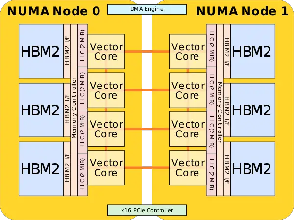
The SX-Aurora supports partitioning mode whereby the vector cores, the last level cache, and the HBM memory stacks are partitioned into two equal NUMA segments. When enabled, the cores in one NUMA node only utilize the LLC and memory allocated to that segment. The effect is that less LLC conflict might occur, however, the memory capacity and overall bandwidth are halved. This model is disabled by default, however, in some situations, certain applications might see better performance.
Package[edit]
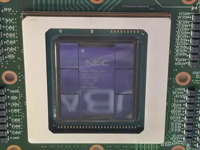
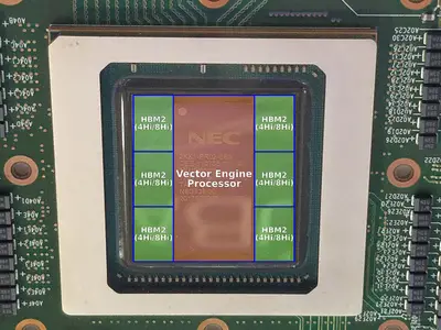
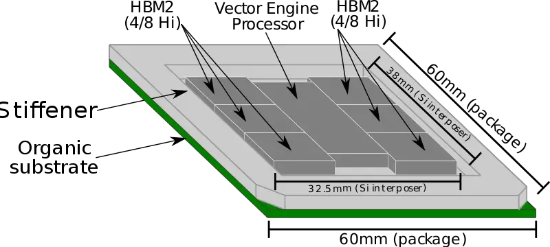
The SX-Aurora chip uses six HBM2 stacks. Those are either 4 Hi or 8 Hi stacks. The chip utilizes TSMC's second-generation chip on wafer on substrate (CoWoS) technology with NEC's implementation developed in collaboration with TSMC and Broadcom. This chip became the world's first to utilize six HBM2s.
The package itself is very big at 60 mm x 60 mm. The VE processor die itself is 15 mm x 33 mm with a very large interposer with a total Si area of 1,235 mm² (32.5 mm x 38 mm).
Though other chips have reached very large interposer sizes before, the SX-Aurora is the first 6 HBM2 implementation. It uses the second-generation CoWoS packaging technology (CoWoS-XL2) to exceed the reticle size through the use of mask stitching.
All SX-Aurora Chips[edit]
| List of SX-Aurora-based Vector Engine Processors | |||||||
|---|---|---|---|---|---|---|---|
| Vector Processor | HBM2 | ||||||
| Model | Launched | Cores | L3$ | Frequency | Performance | Memory | Bandwidth |
| Type 10A | 2018 | 8 | 16 MiB 16,384 KiB 16,777,216 B 0.0156 GiB | 1.6 GHz 1,600 MHz 1,600,000 kHz | 2.46 teraFLOPS 2,460,000,000,000 FLOPS 2,460,000,000 KFLOPS 2,460,000 MFLOPS 2,460 GFLOPS 0.00246 PFLOPS | 48 GiB 49,152 MiB 50,331,648 KiB 51,539,607,552 B 0.0469 TiB | 1,229 GB/s 1,144.595 GiB/s 1,172,065.735 MiB/s 1,229,000 MB/s 1.118 TiB/s 1.229 TB/s |
| Type 10AE | January 2020 | 8 | 16 MiB 16,384 KiB 16,777,216 B 0.0156 GiB | 1.584 GHz 1,584 MHz 1,584,000 kHz | 2.433 teraFLOPS 2,433,000,000,000 FLOPS 2,433,000,000 KFLOPS 2,433,000 MFLOPS 2,433 GFLOPS 0.00243 PFLOPS | 48 GiB 49,152 MiB 50,331,648 KiB 51,539,607,552 B 0.0469 TiB | 1,382 GB/s 1,287.088 GiB/s 1,317,977.905 MiB/s 1,382,000 MB/s 1.257 TiB/s 1.382 TB/s |
| Type 10B | 2018 | 8 | 16 MiB 16,384 KiB 16,777,216 B 0.0156 GiB | 1.4 GHz 1,400 MHz 1,400,000 kHz | 2.15 teraFLOPS 2,150,000,000,000 FLOPS 2,150,000,000 KFLOPS 2,150,000 MFLOPS 2,150 GFLOPS 0.00215 PFLOPS | 48 GiB 49,152 MiB 50,331,648 KiB 51,539,607,552 B 0.0469 TiB | 1,229 GB/s 1,144.595 GiB/s 1,172,065.735 MiB/s 1,229,000 MB/s 1.118 TiB/s 1.229 TB/s |
| Type 10BE | January 2020 | 8 | 16 MiB 16,384 KiB 16,777,216 B 0.0156 GiB | 1.408 GHz 1,408 MHz 1,408,000 kHz | 2.163 teraFLOPS 2,162,700,000,000 FLOPS 2,162,700,000 KFLOPS 2,162,700 MFLOPS 2,162.7 GFLOPS 0.00216 PFLOPS | 48 GiB 49,152 MiB 50,331,648 KiB 51,539,607,552 B 0.0469 TiB | 1,382 GB/s 1,287.088 GiB/s 1,317,977.905 MiB/s 1,382,000 MB/s 1.257 TiB/s 1.382 TB/s |
| Type 10C | 2018 | 8 | 16 MiB 16,384 KiB 16,777,216 B 0.0156 GiB | 1.4 GHz 1,400 MHz 1,400,000 kHz | 2.15 teraFLOPS 2,150,000,000,000 FLOPS 2,150,000,000 KFLOPS 2,150,000 MFLOPS 2,150 GFLOPS 0.00215 PFLOPS | 24 GiB 24,576 MiB 25,165,824 KiB 25,769,803,776 B 0.0234 TiB | 768 GB/s 715.256 GiB/s 732,421.875 MiB/s 768,000 MB/s 0.698 TiB/s 0.768 TB/s |
| Type 10CE | January 2020 | 8 | 16 MiB 16,384 KiB 16,777,216 B 0.0156 GiB | 1.4 GHz 1,400 MHz 1,400,000 kHz | 2.15 teraFLOPS 2,150,000,000,000 FLOPS 2,150,000,000 KFLOPS 2,150,000 MFLOPS 2,150 GFLOPS 0.00215 PFLOPS | 24 GiB 24,576 MiB 25,165,824 KiB 25,769,803,776 B 0.0234 TiB | 998.4 GB/s 929.832 GiB/s 952,148.437 MiB/s 998,400 MB/s 0.908 TiB/s 0.998 TB/s |
| Count: 6 | |||||||
Vector engine (VE) card[edit]
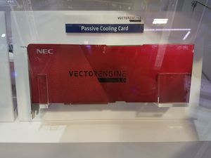
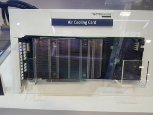
The SX-Aurora chip is part of a complete accelerator card known as the Vector Engine v1. NEC makes those in three variants - passive cooling, active air cooling, and water-cooled.
Die[edit]
- 16 nm process
- 4,800,000,000 transistors
- 14.96 mm x 33.00 mm
- 493.68 mm² die size
Bibliography[edit]
- NEC, IEEE Hot Chips 30 Symposium (HCS) 2018.
- Supercomputing 2018, NEC Aurora Forum
- Supercomputing 2019, NEC
- Some information was obtained directly from NEC
| codename | SX-Aurora + |
| core count | 8 + |
| designer | NEC + |
| first launched | 2018 + |
| full page name | nec/microarchitectures/sx-aurora + |
| instance of | microarchitecture + |
| manufacturer | TSMC + |
| name | SX-Aurora + |
| pipeline stages | 8 + |
