Semiconductor & Computer Engineering
| Edit Values | |
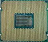
| Skylake (server) µarch | |
| General Info | |
| Arch Type | CPU |
| Designer | Intel |
| Manufacturer | Intel |
| Introduction | May 4, 2017 |
| Process | 14 nm |
| Core Configs | 4, 6, 8, 10, 12, 14, 16, 18, 20, 22, 24, 26, 28 |
| Pipeline | |
| Type | Superscalar |
| OoOE | Yes |
| Speculative | Yes |
| Reg Renaming | Yes |
| Stages | 14-19 |
| Instructions | |
| ISA | x86-16, x86-32, x86-64 |
| Extensions | MOVBE, MMX, SSE, SSE2, SSE3, SSSE3, SSE4.1, SSE4.2, POPCNT, AVX, AVX2, AES, PCLMUL, FSGSBASE, RDRND, FMA3, F16C, BMI, BMI2, VT-x, VT-d, TXT, TSX, RDSEED, ADCX, PREFETCHW, CLFLUSHOPT, XSAVE, SGX, MPX, AVX-512 |
| Cache | |
| L1I Cache | 32 KiB/core 8-way set associative |
| L1D Cache | 32 KiB/core 8-way set associative |
| L2 Cache | 1 MiB/core 16-way set associative |
| L3 Cache | 1.375 MiB/core 11-way set associative |
| Cores | |
| Core Names | Skylake X, Skylake SP |
| Succession | |
Skylake (SKL) Server Configuration is Intel's successor to Broadwell, an enhanced 14nm+ process microarchitecture for enthusiasts and servers. Skylake succeeded Broadwell. Skylake is the "Architecture" phase as part of Intel's PAO model. The microarchitecture was developed by Intel's R&D center in Haifa, Israel.
For desktop enthusiasts, Skylake is branded Core i7, and Core i9 processors (under the Core X series). For scalable server class processors, Intel branded it as Xeon Bronze, Xeon Silver, Xeon Gold, and Xeon Platinum.
There are a fair number of major differences in the Skylake server configuration vs the client configuration.
Contents
- 1 Codenames
- 2 Brands
- 3 Release Dates
- 4 Process Technology
- 5 Compatibility
- 6 Compiler support
- 7 Architecture
- 8 Overview
- 9 Core
- 10 New Technologies
- 11 Mesh Architecture
- 12 Scalability
- 13 Integrated Omni-Path
- 14 Sockets/Platform
- 15 Die
- 16 See also
Codenames
- See also: Client Skylake's Codenames
| Core | Abbrev | Target |
|---|---|---|
| Skylake X | SKL-X | High-end desktops & enthusiasts market |
| Skylake SP | SKL-SP | Server Scalable Processors |
Brands
- See also: Client Skylake's Brands

Intel introduced a number of new server chip families with the introduction of Skylake SP as well as a new enthusiasts family with the introduction of Skylake X.
| Logo | Family | General Description | Differentiating Features | ||||||
|---|---|---|---|---|---|---|---|---|---|
| Cores | HT | AVX | AVX2 | AVX-512 | TBT | ECC | |||
| |
Core i7 | Enthusiasts/High Performance (X) | 6 - 8 | ✔ | ✔ | ✔ | ✔ | ✔ | ✘ |
| |
Core i9 | Enthusiasts/High Performance | 10 - 18 | ✔ | ✔ | ✔ | ✔ | ✔ | ✘ |
| Logo | Family | General Description | Differentiating Features | ||||||
| Cores | HT | TBT | AVX-512 | AVX-512 Units | UPI links | Scalability | |||
.png) |
Xeon Bronze | Entry-level performance / Cost-sensitive |
6 - 8 | ✘ | ✘ | ✔ | 1 | 2 | Up to 2 |
.png) |
Xeon Silver | Mid-range performance / Efficient lower power |
4 - 12 | ✔ | ✔ | ✔ | 1 | 2 | Up to 2 |
.png) |
Xeon Gold 5000 | High performance | 4 - 14 | ✔ | ✔ | ✔ | 1 | 2 | Up to 4 |
| Xeon Gold 6000 | Higher performance | 6 - 22 | ✔ | ✔ | ✔ | 2 | 3 | Up to 4 | |
.png) |
Xeon Platinum | Highest performance / flexibility | 4 - 28 | ✔ | ✔ | ✔ | 2 | 3 | Up to 8 |
Release Dates
Skylake-based Core X was introduced in May 2017 while Skylake SP was introduced in July 2017.
Process Technology
- Main article: Kaby Lake § Process Technology
Unlike mainstream Skylake models, all Skylake server configuration models are fabricated on Intel's enhanced 14+ nm process which is used by Kaby Lake (see Kaby Lake § Process Technology for more info).
Compatibility
| Vendor | OS | Version | Notes |
|---|---|---|---|
| Microsoft | Windows | Windows Server 2008 | Support |
| Windows Server 2008 R2 | |||
| Windows Server 2012 | |||
| Windows Server 2012 R2 | |||
| Windows Server 2016 | |||
| Linux | Linux | Kernel 3.19 | Initial Support (MPX support) |
Compiler support
| Compiler | Arch-Specific | Arch-Favorable |
|---|---|---|
| ICC | -march=skylake-avx512 |
-mtune=skylake-avx512
|
| GCC | -march=skylake-avx512 |
-mtune=skylake-avx512
|
| LLVM | -march=skylake-avx512 |
-mtune=skylake-avx512
|
| Visual Studio | /arch:AVX2 |
/tune:skylake
|
CPUID
| Core | Extended Family |
Family | Extended Model |
Model |
|---|---|---|---|---|
| X | 0 | 0x6 | 0x5 | 0xE |
| Family 6 Model 94 | ||||
| SP | 0 | 0x6 | 0x5 | 0x5 |
| Family 6 Model 85 | ||||
Architecture
Skylake server configuration introduces a number of significant changes from both Intel's previous microarchitecture, Broadwell, as well as the Skylake (client) architecture. Unlike client models, Skylake servers and HEDT models will still incorporate the fully integrated voltage regulator (FIVR) on-die. Those chips also have an entirely new multi-core architecture along with a new mesh topology interconnect network (from ring topology).
Key changes from Broadwell

- Improved "14 nm+" process (see Kaby Lake § Process Technology)
- Omni-Path Architecture (OPA)
- Mesh architecture
- Sub-NUMA Clustering (SNC) support (replaces the Cluster-on-Die (COD) implementation)
- Chipset
- Core
- Front End
- LSD is disabled (Likely due to a bug)
- Larger legacy pipeline delivery (5 µOPs, up from 4)
- Another simple decoder has been added.
- Allocation Queue (IDQ)
- Larger delivery (6 µOPs, up from 4)
- 2.28x larger buffer (64/thread, up from 56)
- Partitioned for each active threads (from unified)
- Improved branch prediction unit
- reduced penalty for wrong direct jump target
- No specifics were disclosed
- µOP Cache
- instruction window is now 64 Bytes (from 32)
- 1.5x bandwidth (6 µOPs/cycle, up from 4)
- Execution Engine
- Larger re-order buffer (224 entries, up from 192)
- Larger scheduler (97 entries, up from 64)
- Larger Integer Register File (180 entries, up from 168)
- Back-end
- Port 4 now performs 512b stores (from 256b)
- Port 0 & Port 1 can now be fused to perform AVX-512
- Port 5 now can do full 512b operations (not on all models)
- Memory Subsystem
- Larger store buffer (56 entries, up from 42)
- Page split load penalty reduced 20-fold
- Larger Write-back buffer
- Store is now 64B/cycle (from 32B/cycle)
- Load is now 2x64B/cycle (from 2x32B/cycle)
- Front End
- Memory
- L2$
- Increased to 1 MiB/core (from 250 KiB/core)
- L3$
- Was made non-inclusive (from inclusive)
- Reduced to 1.375 MiB/core (from 2.5 MiB/core)
- DRAM
- hex-channel DDR4-2666 (from quad-channel)
- L2$
- Support for faster DDR-2666 memory
- TLBs
- ITLB
- 4 KiB page translations was changed from 4-way to 8-way associative
- STLB
- 4 KiB + 2 MiB page translations was changed from 6-way to 12-way associative
- DMI/PEG are now on a discrete clock domain with BCLK sitting on its own domain with full-range granularity (1 MHz intervals)
- ITLB
- Testability
- New support for Direct Connect Interface (DCI), a new debugging transport protocol designed to allow debugging of closed cases (e.g. laptops, embedded) by accessing things such as JTAG through any USB 3 port.
CPU changes
- Most ALU operations have 4 op/cycle 1 for 8 and 32-bit registers. 64-bit ops are still limited to 3 op/cycle. (16-bit throughput varies per op, can be 4, 3.5 or 2 op/cycle).
- MOVSX and MOVZX have 4 op/cycle throughput for 16->32 and 32->64 forms, in addition to Haswell's 8->32, 8->64 and 16->64 bit forms.
- ADC and SBB have throughput of 1 op/cycle, same as Haswell.
- Vector moves have throughput of 4 op/cycle (move elimination).
- Not only zeroing vector vpXORxx and vpSUBxx ops, but also vPCMPxxx on the same register, have throughput of 4 op/cycle.
- Vector ALU ops are often "standardized" to latency of 4. for example, vADDPS and vMULPS used to have L of 3 and 5, now both are 4.
- Fused multiply-add ops have latency of 4 and throughput of 0.5 op/cycle.
- Throughput of vADDps, vSUBps, vCMPps, vMAXps, their scalar and double analogs is increased to 2 op/cycle.
- Throughput of vPSLxx and vPSRxx with immediate (i.e. fixed vector shifts) is increased to 2 op/cycle.
- Throughput of vANDps, vANDNps, vORps, vXORps, their scalar and double analogs, vPADDx, vPSUBx is increased to 3 op/cycle.
- vDIVPD, vSQRTPD have approximately twice as good throughput: from 8 to 4 and from 28 to 12 cycles/op.
- Throughput of some MMX ALU ops (such as PAND mm1, mm2) is decreased to 2 or 1 op/cycle (users are expected to use wider SSE/AVX registers instead).
New instructions
- See also: Client Skylake's New instructions
Skylake server introduced a number of new instructions:
-
SGX1- Software Guard Extensions, Version 1 -
MPX-Memory Protection Extensions -
XSAVEC- Save processor extended states with compaction to memory -
XSAVES- Save processor supervisor-mode extended states to memory. -
CLFLUSHOPT- Flush & Invalidates memory operand and its associated cache line (All L1/L2/L3 etc..) -
AVX-512, specifically: -
PKU- Memory Protection Keys for Userspace -
PCOMMIT- PCOMMIT instruction -
CLWB- CLWB instruction
Block Diagram
Entire SoC Overview
Note that the LCC die is identical without the two bottom rows. The XCC (28-core) die has one additional row and two additional columns of cores. Otherwise the die is identical.

- CHA - Caching and Home Agent
- SF - Snooping Filter
Individual Core

Memory Hierarchy

Some major organizational changes were done to the cache hierarchy in Skylake server configuration vs Broadwell/Haswell. The memory hierarchy for Skylake's server and HEDT processors has been rebalanced. Note that the L3 is now non-inclusive and some of the SRAM from the L3 cache was moved into the private L2 cache.
- Cache
- L0 µOP cache:
- 1,536 µOPs, 8-way set associative
- 32 sets, 6-µOP line size
- statically divided between threads, per core, inclusive with L1I
- 1,536 µOPs, 8-way set associative
- L1I Cache:
- 32 KiB, 8-way set associative
- 64 sets, 64 B line size
- shared by the two threads, per core
- 32 KiB, 8-way set associative
- L1D Cache:
- 32 KiB, 8-way set associative
- 64 sets, 64 B line size
- shared by the two threads, per core
- 4 cycles for fastest load-to-use (simple pointer accesses)
- 5 cycles for complex addresses
- 128 B/cycle load bandwidth
- 64 B/cycle store bandwidth
- Write-back policy
- L2 Cache:
- Unified, 1 MiB, 16-way set associative
- 64 B line size
- Non-inclusive
- 64 B/cycle bandwidth to L1$
- Write-back policy
- 14 cycles latency
- L3 Cache:
- 1.375 MiB/s, shared across all cores
- Note that some models have non-default cache sizes which are larger due to some disabled cores
- 64 B line size
- 11-way set associative
- Non-Inclusive
- Write-back policy
- 50-70 cycles latency
- 1.375 MiB/s, shared across all cores
- L0 µOP cache:
Skylake TLB consists of dedicated L1 TLB for instruction cache (ITLB) and another one for data cache (DTLB). Additionally there is a unified L2 TLB (STLB).
- TLBs:
- ITLB
- 4 KiB page translations:
- 128 entries; 8-way set associative
- dynamic partitioning
- 2 MiB / 4 MiB page translations:
- 8 entries per thread; fully associative
- Duplicated for each thread
- 4 KiB page translations:
- DTLB
- 4 KiB page translations:
- 64 entries; 4-way set associative
- fixed partition
- 2 MiB / 4 MiB page translations:
- 32 entries; 4-way set associative
- fixed partition
- 1G page translations:
- 4 entries; fully associative
- fixed partition
- 4 KiB page translations:
- STLB
- 4 KiB + 2 MiB page translations:
- 1536 entries; 12-way set associative
- fixed partition
- 1 GiB page translations:
- 16 entries; 4-way set associative
- fixed partition
- 4 KiB + 2 MiB page translations:
- ITLB
Overview
Skylake-based servers have been entirely re-architected to meet the need for increased scalabiltiy and performance all while meeting power requirements. A superset model is shown on the right. Skylake-based servers are the first mainstream servers to make use of Intel's new mesh interconnect architecture, an architecture that was previously explored, experimented with, and enhanced with Intel's Phi many-core processors. Those processors are offered from 4 cores up to 28 cores with 8 to 56 threads. With Skylake, Intel now has a separate core architecture for those chips which incorporate a plethora of new technologies and features including support for the new AVX-512 instruction set extension.
All models incorporate 6 channels of DDR4 supporting up to 12 DIMMS for a total of 768 GiB (with extended models support 1.5 TiB). For I/O all models incorporate 48x (3x16) lanes of PCIe 3.0. There is an additional x4 lanes PCIe 3.0 reserved exclusively for DMI for the the Lewisburg chipset. For a selected number of models (specifically those with F suffix) have an Omni-Path Host Fabric Interface (HFI) on-package (see Integrated Omni-Path).
Skylake processors are designed for scalability, supporting 2-way, 4-way, and 8-way multiprocessing through Intel's new Ultra Path Interconnect (UPI) interconnect links, with two to three links being offered (see § Scalability). High-end models have node controller support allowing higher way (e.g., 32-way multiprocessing).
Core
Overview
Skylake shares most of the development vectors with its predecessor while introducing a one of new constraint. The overall goals were:
- Performance improvements - the traditional way of milking more performance by increasing the instructions per cycle as well as clock frequency.
- Power efficiency - reduction of power for all functional blocks
- Security enhancements - new security features are implemented in hardware in the core
- Configurability
Configurability

Intel has been experiencing a growing divergence in functionality over the last number of iterations of their microarchitecture between their mainstream consumer products and their high-end HPC/server models. Traditionally, Intel has been using the same exact core design for everything from their lowest end value models (e.g. Celeron) all the way up to the highest-performance enterprise models (e.g. Xeon E7). While the two have fundamentally different chip architectures, they use the same exact CPU core architecture as the building block.
This design philosophy has changed with Skylake. In order to better accommodate the different functionalities of each segment without sacrificing features or making unnecessary compromises Intel went with a configurable core. The Skylake core is a single development project, making up a master superset core. The project result in two derivatives: one for servers (the substance of this article) and one for clients. All mainstream models (from Celeron/Pentium all the way up to Core i7/Xeon E3) use the client core configuration. Server models (e.g. Xeon Gold/Xeon Platinum) are using the new server configuration instead.
The server core is considerably larger than the client one, featuring Advanced Vector Extensions 512 (AVX-512). Skylake servers support what was formerly called AVX3.2 (AVX512F + AVX512CD + AVX512BW + AVX512DQ + AVX512VL). Additionally, those processors Memory Protection Keys for Userspace (PKU), PCOMMIT, and CLWB.
Pipeline
The Skylake core focuses on extracting performance and reducing power through a number of key ways. Intel builds Skylake on previous microarchitectures, descendants of Sandy Bridge. For the core to increase the overall performance, Intel focused on extracting additional parallelism.
Broad Overview
At a 5,000 foot view, Skylake represents the logical evolution from Haswell and Broadwell. Therefore, despite some significant differences from the previous microarchitecture, the overall designs is fundamentally the same and can be seen as enhancements over Broadwell rather than a complete change.

The pipeline can be broken down into three areas: the front-end, back-end or execution engine, and the memory subsystem. The goal of the front-end is to feed the back-end with a sufficient stream of operations which it gets by decoding instructions coming from memory. The front-end has two major pathways: the µOPs cache path and the legacy path. The legacy path is the traditional path whereby variable-length x86 instructions are fetched from the level 1 instruction cache, queued, and consequently get decoded into simpler, fixed-length µOPs. The alternative and much more desired path is the µOPs cache path whereby a cache containing already decoded µOPs receives a hit allowing the µOPs to be sent directly to the decode queue.
Regardless of which path an instruction ends up taking it will eventually arrive at the decode queue. The IDQ represents the end of the front-end and the in-order part of the machine and the start of the execution engine which operates out-of-order.
In the back-end, the micro-operations visit the reorder buffer. It's there where register allocation, renaming, and retiring takes place. At this stage a number of other optimizations are also done. From the reorder buffer, µOPs are sent to the unified scheduler. The scheduler has a number of exit ports, each wired to a set of different execution units. Some units can perform basic ALU operations, others can do multiplication and division, with some units capable of more complex operations such as various vector operations. The scheduler is effectively in charge of queuing the µOPs on the appropriate port so they can be executed by the appropriate unit.
Some µOPs deal with memory access (e.g. load & store). Those will be sent on dedicated scheduler ports that can perform those memory operations. Store operations go to the store buffer which is also capable of performing forwarding when needed. Likewise, Load operations come from the load buffer. Skylake features a dedicated 32 KiB level 1 data cache and a dedicated 32 KiB level 1 instruction cache. It also features a core-private 1 MiB L2 cache that is shared by both of the L1 caches.
Each core enjoys a slice of a third level of cache that is shared by all the core. In the client configuration for Skylake, there are either two cores or four cores connected while in the server configuration, up to 28 cores may be hooked together on a single chip.
Front-end
The front-end is is tasked with the challenge of fetching the complex x86 instructions from memory, decoding them, and delivering them to the execution units. In other words, the front end needs to be able to consistently deliver enough µOPs from the instruction code stream to keep the back-end busy. When the back-end is not being fully utilized, the core is not reaching its full performance. A poorly or under-performing front-end will translate directly to a poorly performing core. This challenge is further complicated by various redirection such as branches and the complex nature of the x86 instructions themselves.
Fetch & pre-decoding
On their first pass, instructions should have already been prefetched from the L2 cache and into the L1 cache. The L1 is a 32 KiB, 8-way set associative cache, identical in size and organization to previous generations. Skylake fetching is done on a 16-byte fetch window. A window size that has not changed in a number of generations. Up to 16 bytes of code can be fetched each cycle. Note that fetcher is shared evenly between two thread, so that each thread gets every other cycle. At this point they are still macro-ops (i.e. variable-length x86 architectural instruction). Instructions are brought into the pre-decode buffer for initial preparation.

x86 instructions are complex, variable length, have inconsistent encoding, and may contain multiple operations. At the pre-decode buffer the instructions boundaries get detected and marked. This is a fairly difficult task because each instruction can vary from a single byte all the way up to fifteen. Moreover, determining the length requires inspecting a couple of bytes of the instruction. In addition boundary marking, prefixes are also decoded and checked for various properties such as branches. As with previous microarchitectures, the pre-decoder has a throughput of 6 macro-ops per cycle or until all 16 bytes are consumed, whichever happens first. Note that the predecoder will not load a new 16-byte block until the previous block has been fully exhausted. For example, suppose a new chunk was loaded, resulting in 7 instructions. In the first cycle, 6 instructions will be processed and a whole second cycle will be wasted for that last instruction. This will produce the much lower throughput of 3.5 instructions per cycle which is considerably less than optimal. Likewise, if the 16-byte block resulted in just 4 instructions with 1 byte of the 5th instruction received, the first 4 instructions will be processed in the first cycle and a second cycle will be required for the last instruction. This will produce an average throughput of 2.5 instructions per cycle. Note that there is a special case for length-changing prefix (LCPs) which will incur additional pre-decoding costs. Real code is often less than 4 bytes which usually results in a good rate.
All of this works along with the branch prediction unit which attempts to guess the flow of instructions. In Skylake, the branch predictor has also been improved. The branch predictor now has reduced penalty (i.e. lower latency) for wrong direct jump target prediction. Additionally, the predictor in Skylake can inspect further in the byte stream than in previous architectures. The intimate improvements done in the branch predictor were not further disclosed by Intel.
Instruction Queue & MOP-Fusion
| MOP-Fusion Example: | ||
cmp eax, [mem] jne loop |
→ | cmpjne eax, [mem], loop |
- See also: Macro-Operation Fusion
The pre-decoded instructions are delivered to the Instruction Queue (IQ). In Broadwell, the Instruction Queue has been increased to 25 entries duplicated over for each thread (i.e. 50 total entries). It's unclear if that has changed with Skylake. One key optimization the instruction queue does is macro-op fusion. Skylake can fuse two macro-ops into a single complex one in a number of cases. In cases where a test or compare instruction with a subsequent conditional jump is detected, it will be converted into a single compare-and-branch instruction. Those fused instructions remain fused throughout the entire pipeline and get executed as a single operation by the branch unit thereby saving bandwidth everywhere. Only one such fusion can be performed each cycle.
Decoding

Up to five pre-decoded instructions are sent to the decoders each cycle. Like the fetchers, the Decoders alternate between the two thread each cycle. Decoders read in macro-operations and emit regular, fixed length µOPs. Skylake represents a big genealogical change from the last couple of microarchitectures. Skylake's pipeline is wider than it predecessors; Skylake adds another simple decoder. The five decoders are asymmetric; the first one, Decoder 0, is a complex decoder while the other four are simple decoders. A simple decoder is capable of translating instructions that emit a single fused-µOP. By contrast, a complex decoder can decode anywhere from one to four fused-µOPs. Skylake is now capable of decoding 5 macro-ops per cycle or 25% more than Broadwell, however this does not translates directly to direct IPC uplift to due to various other more restricting points in the pipeline. Intel chose not increase the number of complex decoders because it's much harder to extract additional parallelism from the µOPs emitted by a complex instruction. Overall up to 5 simple instructions can be decoded each cycle with lesser amounts if the complex decoder needs to emit addition µOPs; i.e., for each additional µOP the complex decoder needs to emit, 1 less simple decoder can operate. In other words, for each additional µOP the complex decoder emits, one less decoder is active.
MSROM & Stack Engine
There are more complex instructions that are not trivial to be decoded even by complex decoder. For instructions that transform into more than four µOPs, the instruction detours through the microcode sequencer (MS) ROM. When that happens, up to 4 µOPs/cycle are emitted until the microcode sequencer is done. During that time, the decoders are disabled.
x86 has dedicated stack machine operations. Instructions such as PUSH, POP, as well as CALL, and RET all operate on the stack pointer (ESP). Without any specialized hardware, such operations would would need to be sent to the back-end for execution using the general purpose ALUs, using up some of the bandwidth and utilizing scheduler and execution units resources. Since Pentium M, Intel has been making use of a Stack Engine. The Stack Engine has a set of three dedicated adders it uses to perform and eliminate the stack-updating µOPs (i.e. capable of handling three additions per cycle). Instruction such as PUSH are translated into a store and a subtraction of 4 from ESP. The subtraction in this case will be done by the Stack Engine. The Stack Engine sits after the decoders and monitors the µOPs stream as it passes by. Incoming stack-modifying operations are caught by the Stack Engine. This operation alleviate the burden of the pipeline from stack pointer-modifying µOPs. In other words, it's cheaper and faster to calculate stack pointer targets at the Stack Engine than it is to send those operations down the pipeline to be done by the execution units (i.e., general purpose ALUs).
µOP cache & x86 tax

Decoding the variable-length, inconsistent, and complex x86 instructions is a nontrivial task. It's also expensive in terms of performance and power. Therefore, the best way for the pipeline to avoid those things is to simply not decode the instructions. This is the job of the µOP cache or the Decoded Stream Buffer (DSB). Skylake's µOP cache is organized similarly to previous generations like Sandy Bridge, however both the bandwidth and the tracking window was increased. The cache is organized into 32 sets of 8 cache lines with each line holding up to 6 µOP for a total of 1,536 µOPs. Whereas previously (e.g. Haswell) the µOP cache operated on 32-byte windows, in Skylake the window size has been doubled to 64-bytes. The micro-operation cache is competitively shared between the two threads and can also hold pointers to the microcode. The µOP cache has an average hit rate of 80%.
A hit in the µOP allows for up to 6 µOP (i.e., entire line) per cycle to be sent directly to the Instruction Decode Queue (IDQ), bypassing all the pre-decoding and decoding that would otherwise have to be done. Whereas the legacy decode path works in 16-byte instruction fetch windows, the µOP cache has no such restriction and can deliver 6 µOP/cycle corresponding to the much bigger 64-byte window. Previously (e.g., Broadwell), the bandwidth was lower at 4 µOP per cycle. The 1.5x bandwidth increase greatly improves the numbers of µOP that the back-end can take advantage of in the out-of-order part of the machine.
Allocation Queue
The emitted µOPs from the decoders are sent directly to the Allocation Queue (AQ) or Instruction Decode Queue (IDQ). The Allocation Queue acts as the interface between the front-end (in-order) and the back-end (out-of-order). Skylake's Allocation Queue has more than doubled from Broadwell from 28-entries per thread to 64-entries per thread. Unlike in Haswell, the IDQ is no longer competitively shared; it's partitioned between two active threads. The queue's purpose is effectively help absorb bubbles which may be introduced in the front-end, ensuring that a steady stream of 6 µOPs are delivered each cycle.
µOP-Fusion & LSD
The Loop Stream Detector (LSD) has been disabled. While the exact reason is not known, it might be related to a severe issue that was experienced by the OCaml Development Team. The issue was patched via microcode on the client platform, however this change might indicate it was possibly disabled on there as well. The exact implications of this are unknown.
- The following no longer applies:
The IDQ does a number of additional optimizations as it queues instructions. The Loop Stream Detector (LSD) is a mechanism inside the IDQ capable of detecting loops that fit in the IDQ and lock them down. That is, the LSD can stream the same sequence of µOPs directly from the IDQ continuously without any additional fetching, decoding, or utilizing additional caches or resources. Streaming continues indefinitely until reaching a branch mis-prediction. Note that while the LSD is active, the rest of the front-end is effectively disabled.
The LSD in Skylake can take advantage of the considerably larger IDQ; capable of detecting loops up to 64 µOPs per thread. The LSD is particularly excellent in for many common algorithms that are found in many programs (e.g., tight loops, intensive calc loops, searches, etc..).
Execution engine

Skylake's back-end or execution engine deals with the execution of out-of-order operations. Much of the design is inherited from previous architectures such as Haswell but has been widened to explorer more instruction-level parallelism opportunities. From the allocation queue instructions are sent to the Reorder Buffer (ROB) at the rate of up to 6 fused-µOPs each cycle. Skylake's throughput is up by 2 fused-µOPs per cycle from Broadwell in order to accommodate the wider front-end.
Renaming & Allocation
Like the front-end, the Reorder Buffer has been increased to 224 entries, 32 entries more than Broadwell. It is at this stage that architectural registers are mapped onto the underlying physical registers. Other additional bookkeeping tasks are also done at this point such as allocating resources for stores, loads, and determining all possible scheduler ports. Register renaming is also controlled by the Register Alias Table (RAT) which is used to mark where the data we depend on is coming from (after that value, too, came from an instruction that has previously been renamed). In previous microarchitectures, the RAT could handle 4 µOPs each cycle. Intel has not disclosed if that has changed in Skylake but it's possible. If this has not change, Skylake can rename any four registers per cycle. This includes the same register renamed four times in a single cycle. If the rename has not increased in Skylake, some aspects of improvements that were done in the prefetch/decode stages are effectively lost. Note that the ROB still operates on fused µOPs, therefore 4 µOPs can effectively be as high as 8 µOPs.
It should be noted that there is no special costs involved in splitting up fused µOPs before execution or retirement and the two fused µOPs only occupy a single entry in the ROB.
Since Skylake performs speculative execution, it can speculate incorrectly. When this happens, the architectural state is invalidated and as such needs to be rolled back to the last known valid state. Skylake has a 48-entry Branch Order Buffer (BOB) that keeps tracks of those states for this very purpose.
Optimizations
Skylake as a number of optimizations it performs prior to entering the out-of-order and renaming part. Three of those optimizations include Move Elimination and Zeroing Idioms, and Ones Idioms. A Move Elimination is capable of eliminating register-to-register moves (including chained moves) prior to bookkeeping at the ROB, allowing those µOPs to save resources and eliminating them entirely. Eliminated moves are zero latency and are entirely removed from the pipeline. This optimization does not always succeed; when it fails, the operands were simply not ready. On average this optimization is almost always successful (upward of 85% in most cases). Move elimination works on all 32- and 64-bit GP integer registers as well as all 128- and 256-bit vector registers.
| Zeroing Idiom Example: |
xor eax, eax |
Not only does this instruction get eliminated at the ROB, but it's actually encoded as just 2 bytes 31 C0 vs the 4 bytes for mov eax, 0x0 which is encoded as b8 00 00 00 00.
|
There are some exceptions that Skylake will not optimize, most dealing with signedness. sign-extended moves cannot be eliminated and neither can zero-extended from 16-bit to 32/64 big registers (note that 8-bit to 32/64 works). Likewise, in the other direction, no moves to 8/16-bit registers can be eliminated. A move of a register to itself is never eliminated.
When instructions use registers that are independent of their prior values, another optimization opportunity can be exploited. A second common optimization performed in Skylake around the same time is Zeroing Idioms elimination. A number common zeroing idioms are recognized and consequently eliminated in much the same way as the move eliminations are performed. Skylake recognizes instructions such as XOR, PXOR, and XORPS as zeroing idioms when the source and destination operands are the same. Those optimizations are done at the same rate as renaming during renaming (at 4 µOPs per cycle) and the register is simply set to zero.
The ones idioms is another dependency breaking idiom that can be optimized. In all the various PCMPEQx instructions that perform packed comparison the same register with itself always set all bits to one. On those cases, while the µOP still has to be executed, the instructions may be scheduled as soon as possible because all the decencies are resolved.
Scheduler

The scheduler itself was increased by 50%; with up to 97 entries (from 64 in Broadwell) being competitively shared between the two threads. Skylake continues with a unified design; this is in contrast to designs such as AMD's Zen which uses a split design each one holding different types of µOPs. Scheduler includes the two register files for integers and vectors. It's in those register files that output operand data is store. In Skylake, the integer register file was also slightly increased from 160 entries to 180.
At this point µOPs are not longer fused and will be dispatched to the execution units independently. The scheduler holds the µOPs while they wait to be executed. A µOP could be waiting on an operand that has not arrived (e.g., fetched from memory or currently being calculated from another µOPs) or because the execution unit it needs is busy. Once the µOP is ready, they are dispatched through their designated port. The scheduler will send the oldest ready µOP to be executed on each of the eight ports each cycle.
The scheduler had its ports rearranged to better balance various instructions. For example, divide and sqrt instructions latency and throughput were improved. The latency and throughput of floating point ADD, MUL, and FMA were made uniformed at 4 cycles with a throughput of 2 µOPs/clock. Likewise the latency of AES instructions were significantly reduced from 7 cycles down to 4.
512-SIMD addition

This is the first implementation to incorporate AVX-512, a 512-bit SIMD x86 instruction set extension. Intel introduced AVX-512 in two different ways:
In the simple implementation, the variants used in the entry-level and mid-range Xeon servers, AVX-512 fuses Port 0 and Port 1 to form a 512-bit unit. Since those two ports are 256-wide, an AVX-512 option that is dispatched by the scheduler to port 0 will execute on both ports. Note that unrelated operations can still execute in parallel. For example, an AVX-512 operation and an Int ALU operation may execute in parallel - the AVX-512 is dispatched on port 0 and use the AVX unit on port 1 as well and the Int ALU operation will execute independently in parallel on port 1.
In the high-end and highest performance Xeons, Intel added a second dedicated AVX-512 unit in addition to the fused Port0-1 operations described above. The dedicated unit is situated on Port 5.
Physically, Intel added 768 KiB L2 cache and the second AVX-512 VPU externally to the core.
Scheduler Ports & Execution Units
| Scheduler Ports Designation | ||
|---|---|---|
| Port 0 | Integer/Vector Arithmetic, Multiplication, Logic, Shift, and String ops | 512-bit Vect ALU/Shift/Mul/FMA |
| FP Add, Multiply, FMA | ||
| Integer/FP Division and Square Root | ||
| AES Encryption | ||
| Branch2 | ||
| Port 1 | Integer/Vector Arithmetic, Multiplication, Logic, Shift, and Bit Scanning | |
| FP Add, Multiply, FMA | ||
| Port 5 | Integer/Vector Arithmetic, Logic | 512-bit Vect ALU/Shift/Mul/FMA |
| Vector Permute | ||
| x87 FP Add, Composite Int, CLMUL | ||
| Port 6 | Integer Arithmetic, Logic, Shift | |
| Branch | ||
| Port 2 | Load, AGU | |
| Port 3 | Load, AGU | |
| Port 4 | Store, AGU | |
| Port 7 | AGU | |
| Execution Units | ||
|---|---|---|
| Execution Unit | # of Units | Instructions |
| ALU | 4 | add, and, cmp, or, test, xor, movzx, movsx, mov, (v)movdqu, (v)movdqa, (v)movap*, (v)movup* |
| DIV | 1 | divp*, divs*, vdiv*, sqrt*, vsqrt*, rcp*, vrcp*, rsqrt*, idiv |
| Shift | 2 | sal, shl, rol, adc, sarx, adcx, adox, etc... |
| Shuffle | 1 | (v)shufp*, vperm*, (v)pack*, (v)unpck*, (v)punpck*, (v)pshuf*, (v)pslldq, (v)alignr, (v)pmovzx*, vbroadcast*, (v)pslldq, (v)psrldq, (v)pblendw |
| Slow Int | 1 | mul, imul, bsr, rcl, shld, mulx, pdep, etc... |
| Bit Manipulation | 2 | andn, bextr, blsi, blsmsk, bzhi, etc |
| FP Mov | 1 | (v)movsd/ss, (v)movd gpr |
| SIMD Misc | 1 | STTNI, (v)pclmulqdq, (v)psadw, vector shift count in xmm |
| Vec ALU | 3 | (v)pand, (v)por, (v)pxor, (v)movq, (v)movq, (v)movap*, (v)movup*, (v)andp*, (v)orp*, (v)paddb/w/d/q, (v)blendv*, (v)blendp*, (v)pblendd |
| Vec Shift | 2 | (v)psllv*, (v)psrlv*, vector shift count in imm8 |
| Vec Add | 2 | (v)addp*, (v)cmpp*, (v)max*, (v)min*, (v)padds*, (v)paddus*, (v)psign, (v)pabs, (v)pavgb, (v)pcmpeq*, (v)pmax, (v)cvtps2dq, (v)cvtdq2ps, (v)cvtsd2si, (v)cvtss2si |
| Vec Mul | 2 | (v)mul*, (v)pmul*, (v)pmadd* |
| This table was taken verbatim from the Intel manual. Execution unit mapping to MMX instructions are not included. | ||
Retirement
Once a µOP executes, or in the case of fused µOPs both µOPs have executed, they can be retired. Haswell is able to commit up to four fused µOPs each cycle per thread. Retirement happens in-order and releases any used resources such as those used to keep track in the reorder buffer. Because the allocation queue delivery in Skylake has been increased to 6 µOPs (12 unfused) from previously 4 µOPs (8 unfused) per cycle, the SMT implementation in Skylake should have some additional efficiency as there's now better chance for higher sustainable retirement rate.
Memory subsystem

Skylake's memory subsystem is in charge of the loads and store requests and ordering. Since Haswell, it's possible to sustain two memory reads (on ports 2 and 3) and one memory write (on port 4) each cycle. Each memory operation can be of any register size up to 512 bits. Skylake memory subsystem has been improved. The store buffer has been increased by 42 entries from Broadwell to 56 for a total of 128 simultaneous memory operations in-flight or roughly 60% of all µOPs. Special care was taken to reduce the penalty for page-split loads; previously scenarios involving page-split loads were thought to be rarer than they actually are. This was addressed in Skylake with page-split loads are now made equal to other splits loads. Expect page split load penalty down to 5 cycles from 100 cycles in Broadwell. The average latency to forward a load to store has also been improved and stores that miss in the L1$ generate L2$ requests to the next level cache much earlier in Skylake than before.
The L2 to L1 bandwidth in Skylake is the same as Haswell at 64 bytes per cycle in either direction. Note that one operation can be done each cycle; i.e., the L1 can either receive data from the L1 or send data to the Load/Store buffers each cycle, but not both. Latency from L2$ to L3$ has also been increased from 4 cycles/line to 2 cycles/line.
The medium level cache (MLC) and last level cache (LLC) was rebalanced. Traditionally, Intel had a 256 KiB L2 cache which was duplicated along with the L1s over in the LLC which was 2.5 MiB. That is, prior to Skylake, the 256 KiB L2 cache actually took up 512 KiB of space for a total of 2.25 mebibytes effective cache per core. In Skylake Intel doubled the L2 and quadrupled the effective capacity to 1 MiB while decreasing the LLC to 1.375 MiB. The LLC is also now made non-inclusive, i.e., the L2 may or may not be in the L3 (no guarantee is made); what stored where will depend on the particular access pattern of the executing application, the size of code and data accessed, and the inter-core sharing behavior. Having an inclusive L3 makes cache coherence considerably easier to implement. Snooping only requires checking the L3 cache tags to know if the data is on board and in which core. It also makes passing data around a bit more efficient. It's currently unknown what mechanism is being used to reduce snooping. In the past, Intel has discussed a couple of additional options they were researching such as NCID (non-inclusive cache, inclusive directory architecture). It's possible that a NCID is being used in Skylake or a related derivative. These changes also mean that software optimized for data placing in the various caches needs to be revised for the new changes, particularly in situations where data is not shared, the overall capacity can be treated as L2+L3 for a total of 2.375 MiB.
New Technologies
Software Guard Extension (SGX)
- Main article: Intel's Software Guard Extension
Software Guard Extension (SGX) is a new inter-software guard x86 extension that allows software in user-level mode to create isolated secure environments called "enclaves" for storing data or code. Data and code stored in enclaves are protected from external processes including code executing with higher privileges including the operating system or a hypervisor (including all forms of debugging).
Memory Protection Extension (MPX)
- Main article: Intel's Memory Protection Extension
Memory Protection Extension (MPX) is a new x86 extension that offers a hardware-level bound checking implementation. This extension allows an application to define memory boundaries for allocated memory areas. The processors can then check all proceeding memory accesses against those boundaries to ensure accesses are not out of bound. A program accessing a boundary-marked buffer out of buffer will generate an exception.
Key Protection Technology (KPT)
Key Protection Technology (KPT) is designed to help secure sensitive private keys in hardware at runtime. KPT augments QuickAssist Technology (QAT) hardware crypto accelerators with run-time storage of private keys using Intel's existing Platform Trust Technology (PTT), thereby allowing high throughput hardware security acceleration. The QAT accelerators are all integrated onto Intel's new Lewisburg chipset along with the Converged Security Manageability Engine (CSME) which implements Intel's PTT. The CSME is linked through a private hardware link that is invisible to x86 software and simple hardware probes.
Memory Protection Keys for Userspace (PKU)
Memory Protection Keys for Userspace (PKU also PKEYs) is an extension that provides a mechanism for enforcing page-based protections - all without requiring modification of the page tables when an application changes protection domains. PKU introduces 16 keys by re-purposing the 4 ignored bits from the page table entry.
Mode-Based Execute (MBE) Control
Mode-Based Execute (MBE) is an enhancement to the Extended Page Tables (EPT) that provides finer level of control of execute permissions. With MBE the previous Execute Enable (X) bit is turned into Excuse Userspace page (XU) and Execute Supervisor page (XS). The processor selects the mode based on the guest page permission. With proper software support, hypervisors can take advantage of this as well to ensure integrity of kernel-level code.
Mesh Architecture

On the previous number of generations, Intel has been adding cores onto the die and connecting them via a ring architecture. This was sufficient until recently. With each generation, the added cores increased the access latency while lowering the available bandwidth per core. Intel mitigated this problem by splitting up the die into two halves each on its own ring. This reduced hopping distance and added additional bandwidth but it did not solve the growing fundamental inefficiencies of the ring architecture.
This was completely addressed with the new mesh architecture that is implemented in the Skylake server processors. The mesh is arranged as a matrix of vertical and horizontal communication paths which allow communication to take the shortest path to the correct node. The new mesh architecture implements a modular design for the routing resources in order to remove the various bottlenecks. That is, the mesh architecture now integrates the caching agent, the home agent, and the IO subsystem on the mesh interconnect distributed across all the cores. Each core now has its own associated LLC slice as well as the snooping filter and the Caching and Home Agent (CHA). Additional nodes such as the two memory controllers, the Ultra Path Interconnect (UPI) nodes and PCIe are not independent node on the mesh as well and they now behave identically to any other node/core in the network. This means that in addition to the performance increase expected from core-to-core and core-to-memory latency, there should be substantial increase in I/O performance. The CHA which is found on each of the LLC slices now maps addresses being accessed to the specific LLC bank, memory controller, or I/O subsystem. This provides the necessary information required for the routing to take place.
Cache Coherency
Given the new mesh architecture, new tradeoffs were involved. The new UPI inter-socket links are a valuable resource that could bottlenecked when flooded with unnecessary cross-socket snoop requests. There's also considerably higher memory bandwidth with Skylake which can impact performance. As a compromise, the previous four snoop modes (no-snoop, early snoop, home snoop, and directory) have been reduced to just directory-base coherency. This also alleviates the implementation complex (which is already complex enough in itself).

It should be pointed out that the directory-base coherency optimizations that were done in previous generations have been furthered improved with Skylake - particularly OSB, HitME cache, IO directory cache. Skylake maintained support for Opportunistic Snoop Broadcast (OSB) which allows the network to opportunistically make use of the UPI links when idle or lightly loaded thereby avoiding an expensive memory directory lookup. With the mesh network and distributed CHAs, HitME is now distributed and scales with the CHAs, enhancing the speeding up of cache-to-cache transfers (Those are your migratory cache lines that frequently get transferred between nodes). Specifically for I/O operations, the I/O directory cache (IODC), which was introduced with Haswell, improves stream throughput by eliminating directory reads for InvItoE from snoopy caching agent. Previously this was implemented as a 64-entry directory cache to complement the directory in memory. In Skylake, with a distributed CHA at each node, the IODC is implemented as an eight-entry directory cache per CHA.
Sub-NUMA Clustering
In previous generations Intel had a feature called cluster-on-die (COD) which was introduced with Haswell. With Skylake, there's a similar feature called sub-NUMA cluster (SNC). With a memory controller physically located on each side of the die, SNC allows for the creation of two localized domains with each memory controller belonging to each domain. The processor can then map the addresses from the controller to the distributed home ages and LLC in its domain. This allows executing code to experience lower LLC and memory latency within its domain compared to accesses outside of the domain.
It should be pointed out that in contrast to COD, SNC has a unique location for every adddress in the LCC and is evenr duplicated across LLC banks (previously, COD cache lines could have copies). Additionally, on multiprocessor system, address mapped to memory on remote sockets are still uniformally distributed across all LLC banks irrespective of the localized SNC domain.
Scalability
- See also: QuickPath Interconnect and Ultra Path Interconnect
In the last couple of generations, Intel has been utilizing QuickPath Interconnect (QPI) which served as a high-speed point-to-point interconnect. QPI has been replaced the Ultra Path Interconnect (UPI) which is higher-efficiency coherent interconnect for scalable systems, allowing multiple processors to share a single shared address space. Depending on the exact model, each processor can have either either two or three UPI links connecting to the other processors.
UPI links eliminate some of the scalability limited that surfaced in QPI. They use directory-based home snoop coherency protocol and operate at up either 10.4 GT/s or 9.6 GT/s. This is quite a bit different form previous generations. In addition to the various improvements done to the protocol layer, Skylake SP now implements a distributed CHA that is situated along with the LLC bank on each core. It's in charge of tracking the various requests form the core as well as responding to snoop requests from both local and remote agents. The ease of distributing the home agent is a result of Intel getting rid of the requirement on preallocation of resources at the home agent. This also means that future architectures should be able to scale up well.
Depending on the exact model, Skylake processors can scale from 2-way all the way up to 8-way multiprocessing. Note that the high-end models that support 8-way multiprocessing also only come with three UPI links for this purpose while the lower end processors can have either two or three UPI links. Below are the typical configurations for those processors.


Integrated Omni-Path
- See also: Intel's Omni-Path

A number of Skylake SP models (specifically those with the "F" suffix) incorporate the Omni-Path Host Fabric Interface (HFI) on-package. This was previously done with the Knights Landing ("F" suffixed) models. This, in addition to improving cost and power efficiencies, also eliminates the dependency on the x16 PCIe lanes on the motherboard. With the HFI on package, the chip can be plugged in directly to the IFT (Internal Faceplate Transition) carrier via a separate IFP (Internal Faceplate-to-Processor) 1-port cable (effectively a Twinax cable).

Sockets/Platform
Both Skylake X and PS are a two-chip solution linked together via Intel's standard DMI 3.0 bus interface which utilizes 4 PCIe 3.0 lanes (having a transfer rate of 8 GT/s per lane). Skylake SP has additional SMP capabilities which utilizes either 2 or 3 (depending on the model) Ultra Path Interconnect (UPI) links.
| Core | Socket | Permanent | Platform | Chipset | Chipset Bus | SMP Interconnect | |
|---|---|---|---|---|---|---|---|
 |
Skylake X | LGA-2066 | No | 2-chip | Lewisburg | DMI 3.0 | ✘ |
| Skylake SP | LGA-3647 | No | 2-chip + 2-8-way SMP | Lewisburg | DMI 3.0 | UPI |
Packages
| Core | Die Type | Package | Dimensions |
|---|---|---|---|
| Skylake SP | LCC | FCLGA-3647 | 76.16 mm x 56.6 mm |
| HCC | |||
| XCC | |||
| Skylake X | LCC | FCLGA-2066 | 58.5 mm x 51 mm |
| HCC |
Die

Skylake Server class models and high-end desktop (HEDT) consist of 3 different dies: Low Core Count (LCC), High Core Count (HCC), and Extreme Core Count (XCC).
Low Core Count (LCC)
- 14 nm process
- ? metal layers
- ~22.26 mm x ~14.62 mm
- ~325.44 mm² die size
- 10 cores
High Core Count (HCC)
Die shot of the octadeca core HEDT Skylake X processors.
- 14 nm process
- ? metal layers
- ? mm² die size
- 18 cores
.png)
| |
Preliminary Data! Information presented in this article deal with future products, data, features, and specifications that have yet to be finalized, announced, or released. Information may be incomplete and can change by final release. |
_(annotated).png)
Extreme Core Count (XCC)
- 14 nm process
- ? metal layers
- ? mm² die size
- 28 cores

| |
Preliminary Data! Information presented in this article deal with future products, data, features, and specifications that have yet to be finalized, announced, or released. Information may be incomplete and can change by final release. |
.png)
.png)
See also
| codename | Skylake (server) + |
| core count | 4 +, 6 +, 8 +, 10 +, 12 +, 14 +, 16 +, 18 +, 20 +, 22 +, 24 +, 26 + and 28 + |
| designer | Intel + |
| first launched | May 4, 2017 + |
| full page name | intel/microarchitectures/skylake (server) + |
| instance of | microarchitecture + |
| instruction set architecture | x86-16 +, x86-32 + and x86-64 + |
| manufacturer | Intel + |
| microarchitecture type | CPU + |
| name | Skylake (server) + |
| pipeline stages (max) | 19 + |
| pipeline stages (min) | 14 + |
| process | 14 nm (0.014 μm, 1.4e-5 mm) + |