| Edit Values | |
| SX-Aurora µarch | |
| General Info | |
| Arch Type | VPU |
| Designer | NEC |
| Manufacturer | TSMC |
| Introduction | 2018 |
| Core Configs | 8 |
| Pipeline | |
| Type | Superscalar, Pipelined |
| OoOE | Yes |
| Speculative | Yes |
| Reg Renaming | Yes |
| Stages | 8 |
| Decode | 4-way |
| Cache | |
| L1I Cache | 32 KiB/core |
| L1D Cache | 32 KiB/core |
| L2 Cache | 256 KiB/core |
| L3 Cache | 16 MiB/chip |
| Succession | |
SX-Aurora is NEC's successor to the SX-ACE, a 16 nm microarchitecture for vector processors first introduced in 2018.
Contents
History
| This section is empty; you can help add the missing info by editing this page. |
Architecture
Key changes from SX-ACE
- 16 nm process (from 28 nm)
- 1.6x frequency (1.6 GHz, up from 1 GHz)
- 2x vector cores (8, up from 4)
- Vector core
- 1.5x FMAs EUs (3, up from 2)
- 2x VPPs (32, up from 16)
- 3x FLOPs/cycle (192 FLOPs/cycle, up from 64 FLOPs/cycle)
- Memory
This list is incomplete; you can help by expanding it.
Block Diagram
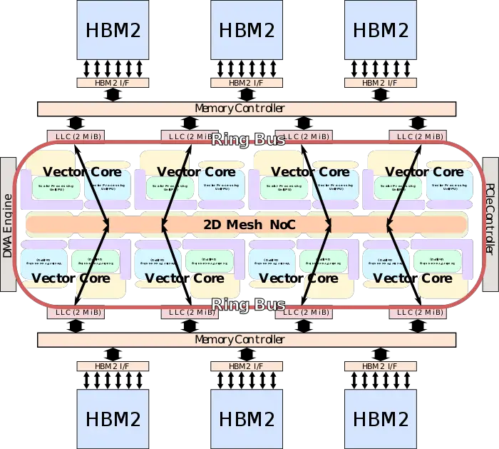
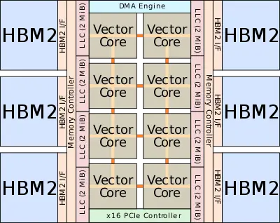
Entire SoC
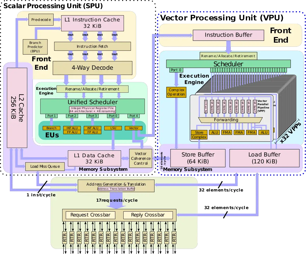
Vector core
Memory Hierarchy
- Vector core
- SPU
- L1I Cache:
- 32 KiB
- L1D Cache:
- 32 KiB
- L2 Cache:
- 256 KiB
- L1I Cache:
- VPU
- 120 KiB load buffer
- 64 KiB store buffer
- SPU
- L3 Cache/LLC:
- 16 MiB
- 8 x 2 MiB
- write-back
- inclusive of L1 & L2
- 128 banks
- 3 TiB/s bandwidth
- 16 MiB
- System DRAM:
Overview
The SX-Aurora is NEC's successor to the SX-ACE, a vector processor designed for high-performance scientific/research applications and supercomputers. The SX-Aurora deviates from all prior chips in the kind of markets it's designed to address. Therefore, NEC made slightly different design choice compared to prior generations of vector processors. In an attempt to broaden their market, NEC extended beyond supercomputers to the conventional server and workstation market. This is done through the use of PCIe-based accelerator cards.
Moving to an accelerator card is not without its challenges. To keep the high memory bandwidth, and thus high bytes per FLOP, while moving a smaller form factor, it was necessary to drop the large amount of DDR memory channels. Instead, NEC opted to utilizing high-bandwidth memory on-chip instead. The card itself is designed to communicate with other cards on the system in order to scale up from just a single card for workstation use to a supercomputer with 64 cards per rack.
The chip itself consists of eight very big cores along with 16 MiB of last level cache on a 2-dimensional mesh. Attached to the LLC are the two memory controllers which interface with the six high-bandwidth memory sitting on an interposer. Fabricated on TSMC's 16 nm process, the SX-Aurora operates at up to 1.6 GHz delivering up to 307.2 gigaFLOPS (double-precision) per core for a total of up to 2.45 teraFLOPS.
Vector core
Like its predecessor, the SX-Aurora vector core itself has three main components - the scalar processing unit (SPU), the vector processing unit (VPU), and the memory subsystem. Though all three were enhanced over the SX-ACE, the emphasis was on the VPU and the new memory subsystem. The majority of the compute capability is in the VPU which can deliver up to 192 DP FLOPS per cycle for up to 307.2 GFLOPS at 1.6 GHz. The VPU is fed by a high-bandwidth mesh capable of 256 B/cycle for a total of up to 410 GB/s for load and store each. The SPU is designed to provide all basic functionalities a typical CPU. Because the SX-Aurora is not a typical offload engine but a self-hosted accelerator, the SPU is designed to deliver high performance to keep pace with the VPU and other operating system-related tasks.
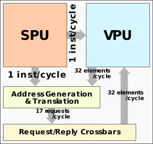
The memory subsystem on the SX-Aurora has been greatly enhanced from the SX-ACE. The primary focus of here is to support contiguous vector memory accesses. To that end, in order to feed the vector pipeline, the address generation unit can receive a vector instruction from the SPU in advance in order to calculate the address and disperse the request to the sixteen ports on the mesh network. 16 elements/cycle vector address generation and translation, as well as 17 requests issued/cycle, can be performed. The bandwidth of the crossbars are matched with the bandwidth of the loads and stores at 256 B/cycle for up to 410 GB/s for load and stores each.
Package
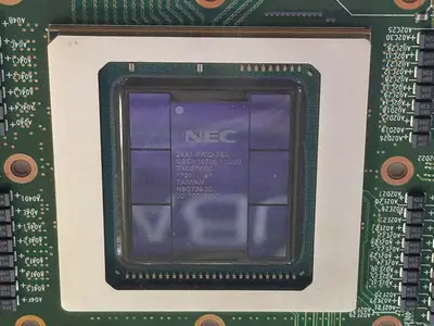
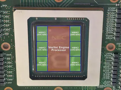
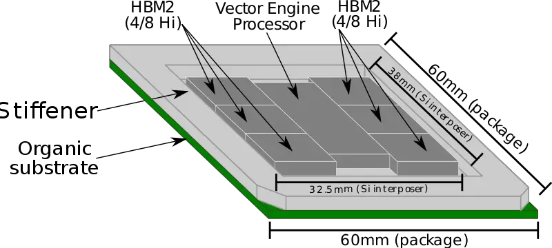
The SX-Aurora chip uses six HBM2 stacks. Those are either 4 Hi or 8 Hi stacks. The chip utilizes TSMC's second-generation chip on wafer on substrate (CoWoS) technology with NEC's implementation developed in collaboration with TSMC and Broadcom. This chip became the world's first to utilize six HBM2s.
The package itself is very big at 60 mm x 60 mm. The VE processor die itself is 15 mm x 33 mm with a very large interposer with a total Si area of 1,235 mm² (32.5 mm x 38 mm).
Though other chips have reached very large interposer sizes before, the SX-Aurora is the first 6 HBM2 implementation. It uses the second-generation CoWoS packaging technology (CoWoS-XL2) to exceed the reticle size through the use of mask stitching.
Vector engine (VE) card
| This section is empty; you can help add the missing info by editing this page. |
Die
- 16 nm process
- 4,800,000,000 transistors
- 14.96 mm x 33.00 mm
- 493.68 mm² die size
Bibliography
- Template:hcbib
- Supercomputing 2018, NEC Aurora Forum
- Some information was obtained directly from NEC
| codename | SX-Aurora + |
| core count | 8 + |
| designer | NEC + |
| first launched | 2018 + |
| full page name | nec/microarchitectures/sx-aurora + |
| instance of | microarchitecture + |
| manufacturer | TSMC + |
| name | SX-Aurora + |
| pipeline stages | 8 + |
