(→Board) |
(→Board) |
||
| Line 115: | Line 115: | ||
== Board == | == Board == | ||
[[File:spring hill board.JPG|right|thumb]] | [[File:spring hill board.JPG|right|thumb]] | ||
| − | [[M.2]] board | + | [[M.2]] board. |
| − | + | <gallery heights=200px widths=700px> | |
| − | + | spring hill m.2 (front).png | |
| + | spring hill m.2 (back).png | ||
| + | </gallery> | ||
== Die == | == Die == | ||
Revision as of 19:38, 12 November 2019
| Edit Values | |
| Spring Hill µarch | |
| General Info | |
| Arch Type | NPU |
| Designer | Intel |
| Manufacturer | Intel |
| Introduction | May, 2019 |
| Process | 10 nm |
| Core Configs | 2 |
| PE Configs | 8, 10, 12 |
| Cache | |
| L3 Cache | 3 MiB/Slice |
Spring Hill (SPH) is a 10 nm microarchitecture designed by Intel for their inference neural processors. Spring Hill was developed by the Israel Haifa Development Center (IDC).
Spring Hill-based products are branded as the NNP-I 1000 series.
Contents
Process technology
Spring Hill NPUs are fabricated on Intel's 10 nm process.
Architecture
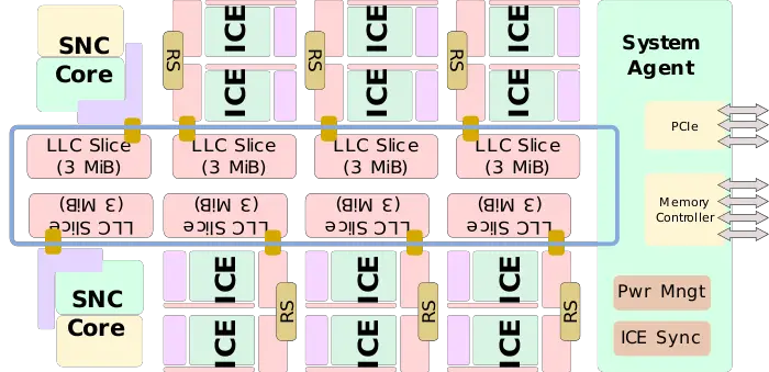
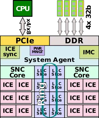
Spring Hill leverages the existing Ice Lake SoC design and makes extensive reuse of IP throughput the chip.
- Uses Ice Lake as the basis for the SoC
- Leverages two Sunny Cove cores
- Leverages the Ring Bus architecture
- Leverages the DVFS power controller
- Leverages the quad-channel 32-bit (128b) LPDDR4x-4200 controller
- Leverages the PCIe controller
- Incorporates 6 pairs of ICEs
- 12 inference and compute units (ICEs)
- 4 MiB Deep SRAM cache
- DL compute grid
- 4K MACs
- Tensilica Vision P6 DSP
- 3 MiB cache slice per pair
- 12 inference and compute units (ICEs)
Block Diagram
SoC Overview
Sunny Cove Core
See Sunny Cove § Block diagram.
Inference Compute Engine
Memory Organization
- Tightly-Coupled Memory (TCM)
- 3 MiB
- 256 KiB/ICE (12 ICEs in total)
- ~68 TB/s
- Deep SRAM
- 48 MiB
- 4 MiB/ICE (12 ICEs in total)
- ~6.8 TB/s
- LLC
- 24 MiB
- 3 MiB/slice (8 slices in total)
- ~680 GB/s
- DRAM
- 32 GiB
- 2x64b or 4x32b LPDDR4x-4200
- 67.2 GB/s
Overview
Spring Hill is Intel's first-generation SoC microarchitecture for neural processors designed for the acceleration of inference in the data center. The design targets data center inference workloads with a performance-power efficiency of close to 5 TOPS/W (4.8 in practice) in a power envelope of 10-50 W in order to main a light PCIe-driven accelerator card form factor such as M.2. The form factor and power envelope is selected for its ease of integration into existing infrastructure without additional cooling/power capacity.
Spring Hill borrows a lot from the client Ice Lake SoC. To that end, Spring Hill features two full-fledge Sunny Cove big cores. The primary purpose of the big cores here is to execute the orchestration software and runtime logic determined by the compiler ahead of time. Additionally, since they come with AVX-512 along with the AVX VNNI extension for inference acceleration, they can be used to run any desired user-specified code, providing an additional layer of programmability. Instead of the traditional integrated graphics and additional cores, Intel integrated up to twelve custom inference compute engines attached to the ring bus in pairs. The ICEs have been designed for inference workloads (see § Inference Compute Engine (ICE)). The ICEs may each be running independent inference workloads or they may be combined to handle larger models faster. Attached to each pair of ICEs and the SNC cores are 3 MiB slices of last level cache for a total of 24 MiB of on-die shared LLC cache. While the LLC is hardware managed, there is some software provisions that can be used to hint the hardware in terms of expectations by dictating service levels and priorities.
In order to simplify the ICE-ICE, ICE-SNC, and even ICE-Host communication, Spring Hill incorporates a special synchronization unit that allows for efficient communication between the units.
Spring Hill borrows a number of other components from Ice Lake including the FIVR and the power management controller which allows the ICEs and SNC to dynamically shift the power to the various execution units depending on the available thermal headroom and the total package power consumption. Various power-related scheduling is also done ahead of time by the compiler. Feeding Spring Hill is a also an LPDDR4x memory controller that supports either dual-channel 64-bit or quad-channel 32-bit (128b in total) with rates up to 4200 MT/s for a total memory bandwidth of 67.2 GB/s.
Inference Compute Engine (ICE)
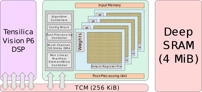
Inference Compute Engines (ICEs) are the individual processing units for inference workloads. Each ICE includes four main components - a DL compute grid, a programmable vector processor, high-bandwidth data scratchpad memory, and a large local SRAM bank. The vector processor is a VP6 DSP designed to provide the ICE with additional programmability support beyond what the compute grid can offer. The vector processor and the compute grid communicate and syncronize using hardware synchronization via the fabric. Additionally, the two processing elements are also tightly connected via the 256 KiB of tightly-coupled memory (TCM).
DL compute grid
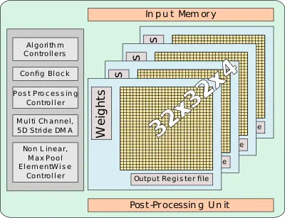
The Deep Learning Compute Grid is a large 4D structure designed to provide 4 ways of parallelism. The grid itself is organized as a 32x32x4 4D grid capable of performing 4K-MAC/cycle (int8). It supports half-precision floating-point (FP16) as well as 8-bit, 4-bit, 2-bit, and even 1-bit precision operations natively. The grid is designed such that data movement is minimized by broadcasting the input data across the entire grid at once. Likewise, within the grid, data reuse is maximized by shifting the data left and right as necessary. This is done through compile-time transformations of the network in order to have a better layout in the hardware.
The compute grid integrates a post-processing unit with hardware-hardened support for various non-linear operations and pooling. The compute grid is managed by a programmable control unit that can map the models in various ways across the grid. The exact way networks are mapped is pre-determined statically are compile-time. Additionally, the control unit can perform various other memory and processing operations.
- DL Compute Grid
- Weights, 1.5 MiB
- Input Feature Maps (IFMs), 384 KiB
- OSRAM, 3 MiB
The compute grid is tightly connected to the high-bandwidth 256 KiB TCM which is also connected to the vector processor.
Programmable vector processor
For additional flexibility, each ICE comes with a customized Cadence Tensilica Vision P6 DSP. This is a 5-slot VLIW 512-bit vector processor configured with two 512-bit vector load ports. It supports FP16 as well as 8-32b integer operations. This DSP was added in order to allow programmable support for operations beyond the ones offered by the compute grid. Intel says that they have customized the DSP with an additional set of custom instructions for the acceleration of various neural network models and various other operations that developers would likely encounter in inference models.
Workload Scalability
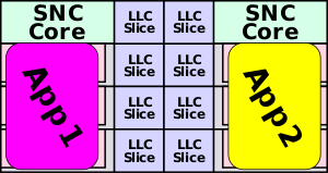
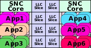
With up to 12 ICEs per chip, depending on the particular nature of the workloads, they may be mapped across a single ICE or multiple. For example, very large models could possibly run across all 12 ICEs in batch 1. Alternatively, smaller workloads may be optimized for throughput instead of latency. In such cases, multiple applications may be mapped across the various ICEs with slightly higher batch sizes.
Board
M.2 board.
Die
- 10 nm process
- 8,500,000,000 transistors
- 239 mm² die size
Bibliography
- Intel, IEEE Hot Chips 30 Symposium (HCS) 2018.
See also
| codename | Spring Hill + |
| core count | 2 + |
| designer | Intel + |
| first launched | May 2019 + |
| full page name | intel/microarchitectures/spring hill + |
| instance of | microarchitecture + |
| manufacturer | Intel + |
| name | Spring Hill + |
| process | 10 nm (0.01 μm, 1.0e-5 mm) + |
| processing element count | 8 +, 10 + and 12 + |
