(→Overview) |
(→Memory controller) |
||
| Line 62: | Line 62: | ||
|bandwidth ochan=63.58 GiB/s | |bandwidth ochan=63.58 GiB/s | ||
}} | }} | ||
| + | |||
| + | *SSD: NVME SSD | ||
| + | * UFS: UFS 3.0 | ||
| + | |||
| + | == DSP == | ||
| + | {{#set: dsp|Hexagon 685 DSP}} | ||
| + | This chip features [[Qualcomm]]'s {{qualcomm|Hexagon}} {{qualcomm|Hexagon 685|685}} DSP. | ||
| + | |||
| + | == Graphics == | ||
| + | {{integrated graphics | ||
| + | | gpu = Adreno 680 GPU | ||
| + | | designer = Qualcomm | ||
| + | | execution units = | ||
| + | | max displays = 3 | ||
| + | | max memory = | ||
| + | | frequency = ? MHz | ||
| + | | max frequency = | ||
| + | |||
| + | | output crt = | ||
| + | | output sdvo = | ||
| + | | output dsi = | ||
| + | | output edp = | ||
| + | | output dp = | ||
| + | | output hdmi = | ||
| + | | output vga = | ||
| + | | output dvi = | ||
| + | |||
| + | | directx ver = 12 | ||
| + | | opengl ver = | ||
| + | | opengl es ver = 3.2 | ||
| + | | opencl ver = 2.0 | ||
| + | | vulkan ver = 1.1 | ||
| + | | hdmi ver = | ||
| + | | dp ver = | ||
| + | | edp ver = | ||
| + | | max res hdmi = | ||
| + | | max res hdmi freq = | ||
| + | | max res dp = | ||
| + | | max res dp freq = | ||
| + | | max res edp = | ||
| + | | max res edp freq = | ||
| + | | max res vga = | ||
| + | | max res vga freq = | ||
| + | }} | ||
| + | |||
| + | * Codec Support: H.265 (HEVC), H.264 (AVC), VP9 | ||
| + | * Playback: Up 4K HDR decode at 120fps | ||
| + | * Capture: | ||
| + | ** 4K Video Capture for Ultra HD Premium Displays (4K@30fps) | ||
| + | ** Slow Motion video capture (720p@480fps) | ||
| + | |||
| + | == Camera == | ||
| + | * ISP | ||
| + | ** Dual 14-bit ISPs | ||
| + | ** Qualcomm Spectra 390 image signal processor | ||
| + | ** Up to 16 MP dual camera | ||
| + | ** Up to 32 MP single camera | ||
| + | |||
| + | == Connectivity == | ||
| + | * X24 LTE modem | ||
| + | ** LTE Category 20 | ||
| + | ** Downlink: | ||
| + | *** 2 Gbps peak | ||
| + | *** 7x20 MHz carrier aggregation | ||
| + | *** Up to 256-QAM | ||
| + | *** Up to 4x4 MIMO on five carriers | ||
| + | *** Full-Dimension MIMO (FD-MIMO) | ||
| + | *** Maximum 20 spatial streams | ||
| + | ** Uplink: | ||
| + | *** 316 Mbps peak | ||
| + | *** 3x20 MHz carrier aggregation | ||
| + | *** Up to 2x 106Mbps LTE streams | ||
| + | *** Up to 256-QAM | ||
| + | *** Uplink data compression | ||
| + | * LTE FDD, LTE TDD including CBRS support, LAA, LTE Broadcast, WCDMA (DB-DC-HSDPA, DC-HSUPA), TD-SCDMA, CDMA 1x, EV-DO, GSM/EDGE | ||
| + | |||
| + | * WiFi | ||
| + | ** Standards: 802.11ad, 802.11ac Wave 2, 802.11a/b/g, 802.11n | ||
| + | ** Spectral Bands: 2.4 GHz, 5 GHz, 60 GHz | ||
| + | ** MIMO Configuration: 2x2 (2-stream) | ||
| + | |||
| + | * Bluetooth | ||
| + | ** Bluetooth 5.0 | ||
| + | |||
| + | == Location == | ||
| + | * Systems: GPS, GLONASS, Beidou, Galileo, QZSS, SBAS | ||
Revision as of 22:32, 6 December 2018
| Edit Values | |
| Snapdragon 8cx | |
 | |
| General Info | |
| Designer | Qualcomm, ARM Holdings |
| Manufacturer | TSMC |
| Market | Mobile |
| Introduction | December 6, 2018 (announced) Q3, 2019 (launched) |
| General Specs | |
| Family | Snapdragon 800 |
| Series | 800 |
| Microarchitecture | |
| ISA | ARMv8 (ARM) |
| Microarchitecture | Cortex-A76, Cortex-A55 |
| Core Name | Cortex-A76, Cortex-A55 |
| Process | 7 nm |
| Technology | CMOS |
| Word Size | 64 bit |
| Cores | 8 |
| Threads | 8 |
| Multiprocessing | |
| Max SMP | 1-Way (Uniprocessor) |
| Electrical | |
| TDP | 7 W |
| Packaging | |
 | |
| Succession | |
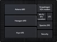
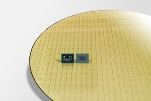
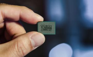
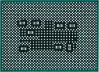
Snapdragon 8cx (Snapdragon 8 Compute eXtreme) is a high-performance 64-bit ARM LTE system on a chip designed by Qualcomm and introduced in late 2018. Fabricated on TSMC's 7nm process, the 8cx features four Kryo 495 Silver high-efficiency cores operating at ? GHz along with two high-performance Kryo 495 Gold operating at ? GHz. The Snapdragon 8cx integrates the Adreno 680 GPU operation at ? MHz and features an X24 LTE modem supporting Cat 20 uplink and Cat 20 downlink. This chip supports up to ? GiB of octa-channel LPDDR4X-4266 memory.
Overview
The Snapdragon 8cx was announced by Qualcomm on December 6, 2018. The chip is what Qualcomm considers a new high tier Snapdragon aimed at always-connected PCs with higher performance and thermal headroom over traditional smartphone devices. The chip comprise of a quad-core cluster of Kryo 495 Gold (Cortex-A76) big cores and a quad-core cluster of Kryo 495 Silver (Cortex-A55) little cores.
Cache
- Main articles: Cortex-A76 § Cache and Cortex-A55
|
Cache Organization
Cache is a hardware component containing a relatively small and extremely fast memory designed to speed up the performance of a CPU by preparing ahead of time the data it needs to read from a relatively slower medium such as main memory. The organization and amount of cache can have a large impact on the performance, power consumption, die size, and consequently cost of the IC. Cache is specified by its size, number of sets, associativity, block size, sub-block size, and fetch and write-back policies. Note: All units are in kibibytes and mebibytes. |
||||||||
|
||||||||
Memory controller
|
Integrated Memory Controller
|
||||||||||||||||||
|
||||||||||||||||||
- SSD: NVME SSD
- UFS: UFS 3.0
DSP
This chip features Qualcomm's Hexagon 685 DSP.
Graphics
|
Integrated Graphics Information
|
||||||||||||||||||||||||||
|
||||||||||||||||||||||||||
- Codec Support: H.265 (HEVC), H.264 (AVC), VP9
- Playback: Up 4K HDR decode at 120fps
- Capture:
- 4K Video Capture for Ultra HD Premium Displays (4K@30fps)
- Slow Motion video capture (720p@480fps)
Camera
- ISP
- Dual 14-bit ISPs
- Qualcomm Spectra 390 image signal processor
- Up to 16 MP dual camera
- Up to 32 MP single camera
Connectivity
- X24 LTE modem
- LTE Category 20
- Downlink:
- 2 Gbps peak
- 7x20 MHz carrier aggregation
- Up to 256-QAM
- Up to 4x4 MIMO on five carriers
- Full-Dimension MIMO (FD-MIMO)
- Maximum 20 spatial streams
- Uplink:
- 316 Mbps peak
- 3x20 MHz carrier aggregation
- Up to 2x 106Mbps LTE streams
- Up to 256-QAM
- Uplink data compression
- LTE FDD, LTE TDD including CBRS support, LAA, LTE Broadcast, WCDMA (DB-DC-HSDPA, DC-HSUPA), TD-SCDMA, CDMA 1x, EV-DO, GSM/EDGE
- WiFi
- Standards: 802.11ad, 802.11ac Wave 2, 802.11a/b/g, 802.11n
- Spectral Bands: 2.4 GHz, 5 GHz, 60 GHz
- MIMO Configuration: 2x2 (2-stream)
- Bluetooth
- Bluetooth 5.0
Location
- Systems: GPS, GLONASS, Beidou, Galileo, QZSS, SBAS
- all microprocessor models
- microprocessor models by qualcomm
- microprocessor models by qualcomm based on cortex-a76
- microprocessor models by qualcomm based on cortex-a55
- microprocessor models by arm holdings
- microprocessor models by arm holdings based on cortex-a76
- microprocessor models by arm holdings based on cortex-a55
- microprocessor models by tsmc
- future microprocessor models
| back image |  + + |
| core count | 8 + |
| core name | Cortex-A76 + and Cortex-A55 + |
| designer | Qualcomm + and ARM Holdings + |
| dsp | Hexagon 685 DSP + |
| family | Snapdragon 800 + |
| first announced | December 6, 2018 + |
| first launched | March 2019 + |
| full page name | qualcomm/snapdragon 800/8cx + |
| has ecc memory support | false + |
| instance of | microprocessor + |
| integrated gpu | Adreno 680 GPU + |
| integrated gpu designer | Qualcomm + |
| isa | ARMv8 + |
| isa family | ARM + |
| l3$ size | 10 MiB (10,240 KiB, 10,485,760 B, 0.00977 GiB) + |
| ldate | 3000 + |
| main image |  + + |
| manufacturer | TSMC + |
| market segment | Mobile + |
| max cpu count | 1 + |
| max memory bandwidth | 29.87 GiB/s (30,586.88 MiB/s, 32.073 GB/s, 32,072.668 MB/s, 0.0292 TiB/s, 0.0321 TB/s) + |
| max memory channels | 8 + |
| microarchitecture | Cortex-A76 + and Cortex-A55 + |
| name | Snapdragon 8cx + |
| process | 7 nm (0.007 μm, 7.0e-6 mm) + |
| series | 800 + |
| smp max ways | 1 + |
| supported memory type | LPDDR4X-4266 + |
| tdp | 7 W (7,000 mW, 0.00939 hp, 0.007 kW) + |
| technology | CMOS + |
| thread count | 8 + |
| word size | 64 bit (8 octets, 16 nibbles) + |
