Semiconductor & Computer Engineering
| Edit Values | |
| Snapdragon 8cx | |
 | |
| General Info | |
| Designer | Qualcomm, ARM Holdings |
| Manufacturer | TSMC |
| Model Number | 8cx |
| Part Number | SC8180X |
| Market | Mobile |
| Introduction | December 6, 2018 (announced) Q3, 2019 (launched) |
| General Specs | |
| Family | Snapdragon 800, Snapdragon 8 |
| Series | 800 |
| Locked | No |
| Frequency | 1.8 GHz, 2.84 GHz |
| Bus speed | 100 MHz |
| Clock multiplier | 28x |
| Microarchitecture | |
| ISA | ARMv8 (ARM) |
| Microarchitecture | Cortex-A55, Cortex-A76 |
| Core Name | Kryo 495 Silver, Kryo 495 Gold |
| Process | 7 nm |
| Technology | CMOS |
| Word Size | 64 bit |
| Cores | 8 |
| Threads | 8 |
| Max Memory | 16 GiB |
| Multiprocessing | |
| Max SMP | 1-Way (Uniprocessor) |
| Electrical | |
| Vcore | 0.5 V-0.95 V |
| TDP | 7 W |
| Packaging | |
 | |
| Succession | |
| Contemporary | |
| Snapdragon 8cx (Gen 2) Snapdragon 8cx (Gen 3) | |
Snapdragon 8cx (Snapdragon 8 Compute eXtreme) is a high-performance 64-bit ARM LTE system on a chip designed by Qualcomm and introduced in late 2018.
Fabricated on TSMC's 7nm process, the 8cx features four Kryo 495 Silver high-efficiency cores operating at 1.8 GHz along with four high-performance Kryo 495 Gold operating at 2.84 GHz.
The Snapdragon 8cx integrates the Adreno 680 GPU operation at 585 MHz and features an X24 LTE modem supporting Cat 20 uplink and Cat 20 downlink. This chip supports up to 16 GiB of octa-channel LPDDR4X-4266 memory.
Contents
Models[edit]
- Snapdragon 8cx (SC8180X) • 7 nm (TSMC N7)
- Kryo 495 Gold/Silver: 4x @2.84GHz Cortex-A76 + 4x @1.80GHz Cortex-A55)
- • Adreno 680 @585 MHz • Hexagon 690 (9 TOPS) • Spectra 390 • Q3 2019
- Snapdragon 8cx (Gen 2 5G) (SC8180XP) • 7 nm (TSMC N7)
- Kryo 495 4 + 4 cores (@3.15GHz Cortex-A76 + @1.8GHz Cortex-A55)
- • Adreno 690 @660MHz • Hexagon 690 (9 TOPS) • Spectra 390 • Q3 2020
- Snapdragon 8cx (Gen 3) (SC8280) • 5 nm (Samsung 5LPE)
- Kryo 4 + 4 cores (@3.0GHz Cortex-X1 + @2.40GHz Cortex-A78)
- • Adreno 695 @900MHz • Hexagon (15 TOPS) • Spectra • Q1 2022
Overview[edit]

The Snapdragon 8cx was announced by Qualcomm on December 6, 2018. The chip is what Qualcomm considers a new high tier Snapdragon aimed at always-connected PCs with higher performance and thermal headroom over traditional smartphone devices. The chip comprise of a quad-core cluster of Kryo 495 Gold (Cortex-A76) big cores and a quad-core cluster of Kryo 495 Silver (Cortex-A55) little cores.
Images[edit]


Cache[edit]
- Main articles: Cortex-A76 § Cache and Cortex-A55
|
Cache Organization
Cache is a hardware component containing a relatively small and extremely fast memory designed to speed up the performance of a CPU by preparing ahead of time the data it needs to read from a relatively slower medium such as main memory. The organization and amount of cache can have a large impact on the performance, power consumption, die size, and consequently cost of the IC. Cache is specified by its size, number of sets, associativity, block size, sub-block size, and fetch and write-back policies. Note: All units are in kibibytes and mebibytes. |
||||||||
|
||||||||
Memory controller[edit]
|
Integrated Memory Controller
|
||||||||||||||||||
|
||||||||||||||||||
- SSD: NVME SSD
- UFS: UFS 3.0
DSP[edit]
This chip features Qualcomm's Hexagon 685 DSP.
Graphics[edit]
|
Integrated Graphics Information
|
||||||||||||||||||||||||||||
|
||||||||||||||||||||||||||||
- Codec Support: H.265 (HEVC), H.264 (AVC), VP9
- Playback: Up 4K HDR decode at 120fps
- Capture:
- 4K Video Capture for Ultra HD Premium Displays (4K@30fps)
- Slow Motion video capture (720p@480fps)
Camera[edit]
- ISP
- Dual 14-bit ISPs
- Qualcomm Spectra 390 image signal processor
- Up to 16 MP dual camera
- Up to 32 MP single camera
Connectivity[edit]
- X24 LTE modem
- LTE Category 20
- Downlink:
- 2 Gbps peak
- 7x20 MHz carrier aggregation
- Up to 256-QAM
- Up to 4x4 MIMO on five carriers
- Full-Dimension MIMO (FD-MIMO)
- Maximum 20 spatial streams
- Uplink:
- 316 Mbps peak
- 3x20 MHz carrier aggregation
- Up to 2x 106Mbps LTE streams
- Up to 256-QAM
- Uplink data compression
- LTE FDD, LTE TDD including CBRS support, LAA, LTE Broadcast, WCDMA (DB-DC-HSDPA, DC-HSUPA), TD-SCDMA, CDMA 1x, EV-DO, GSM/EDGE
- WiFi
- Standards: 802.11ad, 802.11ac Wave 2, 802.11a/b/g, 802.11n
- Spectral Bands: 2.4 GHz, 5 GHz, 60 GHz
- MIMO Configuration: 2x2 (2-stream)
- Bluetooth
- Bluetooth 5.0
Location[edit]
- Systems: GPS, GLONASS, Beidou, Galileo, QZSS, SBAS
Utilizing devices[edit]
- Snapdragon 8cx • Q3 2019
- Lenovo Flex 5G
- Lenovo Yoga 5G
- Lenovo IdeaPad 5G
- Samsung Galaxy Book S
- Snapdragon 8cx Gen 2 • Q3 2020
- Acer Spin 7
- Dell Inspiron 14
- HP Elite Folio
- Huawei MateBook E Go (LTE)
- Samsung Galaxy Book Go (5G)
- Xiaomi Book S
- Snapdragon 8cx Gen 3 • Q4 2021
- Huawei MateBook E Go (Performance)
- Huawei MateBook E Go (2023) (2.69 GHz)
- Lenovo ThinkPad X13s
- Samsung Galaxy Book 2 Pro 360
Documents[edit]
- all microprocessor models
- microprocessor models by qualcomm
- microprocessor models by qualcomm based on cortex-a55
- microprocessor models by qualcomm based on cortex-a76
- microprocessor models by arm holdings
- microprocessor models by arm holdings based on cortex-a55
- microprocessor models by arm holdings based on cortex-a76
- microprocessor models by tsmc
- future microprocessor models
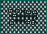
| back image | .png) + + |
| base frequency | 1,800 MHz (1.8 GHz, 1,800,000 kHz) + and 2,840 MHz (2.84 GHz, 2,840,000 kHz) + |
| bus speed | 100 MHz (0.1 GHz, 100,000 kHz) + |
| core count | 8 + |
| core name | Kryo 495 Silver + and Kryo 495 Gold + |
| core voltage (max) | 0.95 V (9.5 dV, 95 cV, 950 mV) + |
| core voltage (min) | 0.5 V (5 dV, 50 cV, 500 mV) + |
| designer | Qualcomm + and ARM Holdings + |
| dsp | Hexagon 685 DSP + |
| family | Snapdragon 800 + and Snapdragon 8 + |
| first announced | December 6, 2018 + |
| first launched | March 2019 + |
| full page name | qualcomm/snapdragon 800/8cx + |
| has ecc memory support | false + |
| has locked clock multiplier | false + |
| instance of | microprocessor + |
| integrated gpu | Adreno 680 GPU + |
| integrated gpu base frequency | 585 MHz (0.585 GHz, 585,000 KHz) + |
| integrated gpu designer | Qualcomm + |
| integrated gpu max frequency | 690 MHz (0.69 GHz, 690,000 KHz) + |
| isa | ARMv8 + |
| isa family | ARM + |
| l3$ size | 10 MiB (10,240 KiB, 10,485,760 B, 0.00977 GiB) + |
| ldate | 3000 + |
| main image | .png) + + |
| manufacturer | TSMC + |
| market segment | Mobile + |
| max cpu count | 1 + |
| max memory | 16,384 MiB (16,777,216 KiB, 17,179,869,184 B, 16 GiB, 0.0156 TiB) + |
| max memory bandwidth | 63.58 GiB/s (65,105.92 MiB/s, 68.269 GB/s, 68,268.505 MB/s, 0.0621 TiB/s, 0.0683 TB/s) + |
| max memory channels | 8 + |
| microarchitecture | Cortex-A55 + and Cortex-A76 + |
| model number | 8cx + |
| name | Snapdragon 8cx + |
| part number | SC8180X + |
| process | 7 nm (0.007 μm, 7.0e-6 mm) + |
| series | 800 + |
| smp max ways | 1 + |
| supported memory type | LPDDR4X-4266 + |
| tdp | 7 W (7,000 mW, 0.00939 hp, 0.007 kW) + |
| technology | CMOS + |
| thread count | 8 + |
| used by | Lenovo Flex 5G +, Lenovo Yoga 5G +, Lenovo IdeaPad 5G +, Samsung Galaxy Book S +, Acer Spin 7 +, Dell Inspiron 14 +, HP Elite Folio +, Huawei MateBook E Go (LTE) +, Samsung Galaxy Book Go (5G) +, Xiaomi Book S +, Huawei MateBook E Go (Performance) +, Huawei MateBook E Go (2023) +, Lenovo ThinkPad X13s + and Samsung Galaxy Book 2 Pro 360 + |
| word size | 64 bit (8 octets, 16 nibbles) + |
.png)
.png)