From WikiChip
Difference between revisions of "movidius/microarchitectures/shave v3.0"
(→Overview) |
(→Key changes from {{\\|SHAVE v2.0}}) |
||
| Line 32: | Line 32: | ||
* [[28 nm process]] (from [[65 nm]]) | * [[28 nm process]] (from [[65 nm]]) | ||
* 20-30x performance | * 20-30x performance | ||
| − | ** | + | ** 600 MHz (3.33x, from 180 MHz) |
** 12 SHAVE cores (from 8) | ** 12 SHAVE cores (from 8) | ||
| − | ** | + | ** Various per-core performance improvement |
| + | * 20 new hardware accelerators | ||
* Aggregate nominal 600 Mpixel/sec throughput | * Aggregate nominal 600 Mpixel/sec throughput | ||
* [[LEON4]] [[SPARC]] core (from [[LEON3]]) | * [[LEON4]] [[SPARC]] core (from [[LEON3]]) | ||
Latest revision as of 04:49, 16 March 2018
| Edit Values | |
| SHAVE v3.0 µarch | |
| General Info | |
| Arch Type | Accelerator |
| Designer | Movidius |
| Manufacturer | TSMC |
| Introduction | 2014 |
| Process | 28 nm |
| Pipeline | |
| Type | VLLIW |
| Instructions | |
| ISA | SHAVE, SPARC v8 |
| Cache | |
| L2 Cache | 256 KiB/chip 2-way set associative |
| Side Cache | 128-256 MiB SDRAM/chip |
| Succession | |
Fragrak or Streaming Hybrid Architecture Vector Engine v3.0 (SHAVE v3.0) is an accelerator microarchitecture designed by Movidius for their vision processors, serving as a successor to the SHAVE v2.0. SHAVE-based products are branded as the Myriad 2 family of vision processors.
Contents
History[edit]
The SHAVE v3.0 microarchitecture is based on the SHAVE v2.0 microarchitecture which Movidius disclosed in 2011. The architecture is a word of a 70-staff team consisting of 65 engineers - 10% working on hardware while the remaining 90% were working on the system tools and software design.
Process Technology[edit]
- Main article: 28 nm lithography process
This microarchitecture was designed for TSMC's 28 nm process.
Architecture[edit]
Key changes from SHAVE v2.0[edit]
- 28 nm process (from 65 nm)
- 20-30x performance
- 600 MHz (3.33x, from 180 MHz)
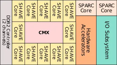
- 12 SHAVE cores (from 8)
- Various per-core performance improvement
- 20 new hardware accelerators
- Aggregate nominal 600 Mpixel/sec throughput
- LEON4 SPARC core (from LEON3)
- Added support for OpenCL
Overview[edit]
Core[edit]
| This section is empty; you can help add the missing info by editing this page. |
Package[edit]
| This section is empty; you can help add the missing info by editing this page. |
Die[edit]
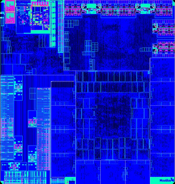
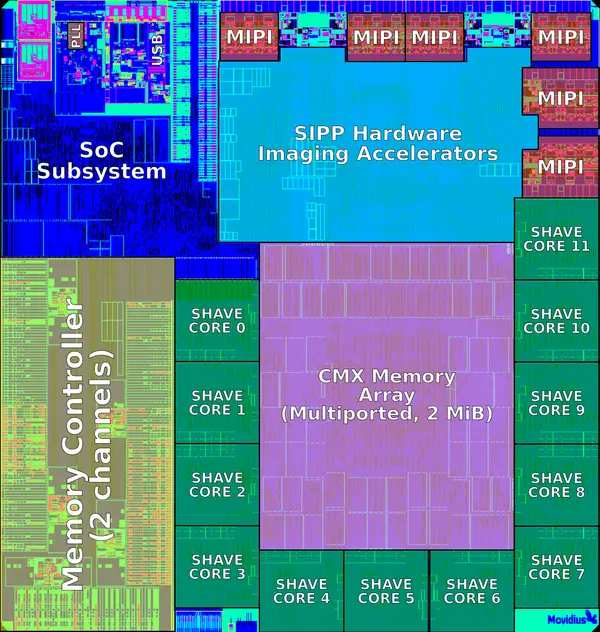
- TSMC's 28HPM process
- 27 mm² die size
| codename | SHAVE v3.0 + |
| designer | Movidius + |
| first launched | 2014 + |
| full page name | movidius/microarchitectures/shave v3.0 + |
| instance of | microarchitecture + |
| instruction set architecture | SHAVE + and SPARC v8 + |
| manufacturer | TSMC + |
| name | SHAVE v3.0 + |
| process | 28 nm (0.028 μm, 2.8e-5 mm) + |


