(→Core) |
|||
| Line 6: | Line 6: | ||
|manufacturer=TSMC | |manufacturer=TSMC | ||
|introduction=2011 | |introduction=2011 | ||
| + | |phase-out=2014 | ||
| + | |process=64 nm | ||
|type=VLIW | |type=VLIW | ||
| + | |isa=SHAVE | ||
| + | |isa 2=SPARC v8 | ||
|l1=1 KiB | |l1=1 KiB | ||
|l1 per=core | |l1 per=core | ||
Revision as of 12:26, 12 March 2018
| Edit Values | |
| SHAVE v2.0 µarch | |
| General Info | |
| Arch Type | Accelerator |
| Designer | Movidius |
| Manufacturer | TSMC |
| Introduction | 2011 |
| Phase-out | 2014 |
| Process | 64 nm |
| Pipeline | |
| Type | VLIW |
| Instructions | |
| ISA | SHAVE, SPARC v8 |
| Cache | |
| L1 Cache | 1 KiB/core |
| L2 Cache | 128 KiB/chip 2-way set associative |
| Side Cache | 8-64 MiB SDRAM/chip |
| Succession | |
Streaming Hybrid Architecture Vector Engine v2.0 (SHAVE v2.0) is an accelerator microarchitecture designed by Movidius for their vision processors. SHAVE-based products are branded as the Myriad family of vision processors.
Contents
History
The original SHAVE architecture was designed primarily for the acceleration of game physics. Low demand for expensive physics acceleration in smartphones has forced to re-focused on image and vision processing. Their architecture was versatile enough that it allowed for fairly simple modification to target machine vision processing.
Process Technology
- Main article: 65 nm lithography process
This microarchitecture was designed for TSMC's 65 nm process.
Architecture
- Hybrid RISC-DSP-GPU VLIW architecture
- 20 GFLOPS computational power
- 180 MHz
- At 300 mW
- Predicated execution
- Branch delay slots
- Tailored to streaming workloads
- 128-bit vector arithmetic
- 8/16/32-bit integer
- 16/32-bit floating point
- Full support for sparse data structures (matrix/array, random access)
Instruction Set
SHAVE supports a mixture of many different types of instructions belonging to a number of different classes of architectures.
- RISC style
- Instruction predication
- Large set of integer operations
- VLIW style
- Parallel functional units controlled by VLIW instructions
- 8/16/32-bit x 1-4 SIMD int
- DSP style
- Zero overhead looping
- Modulo addressing
- Transparent DMA modes
- FFT, Viterbi, etc..
- Parallel comparisons
- GPU style
- Streaming operations
- 16/32-bit FP operations
- Texture management unit
Block Diagram
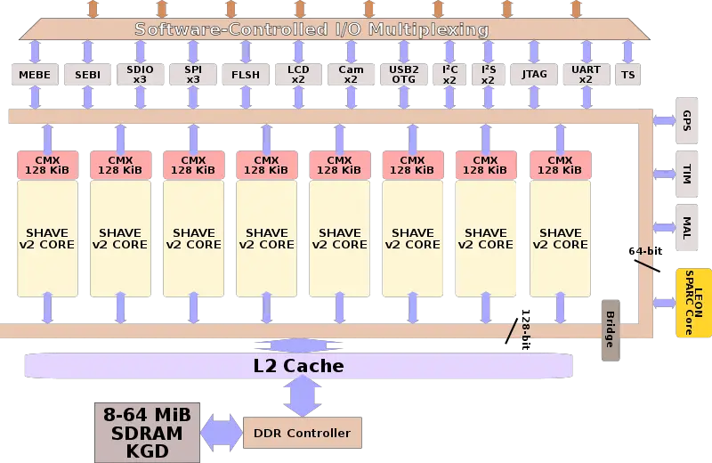
Entire SoC
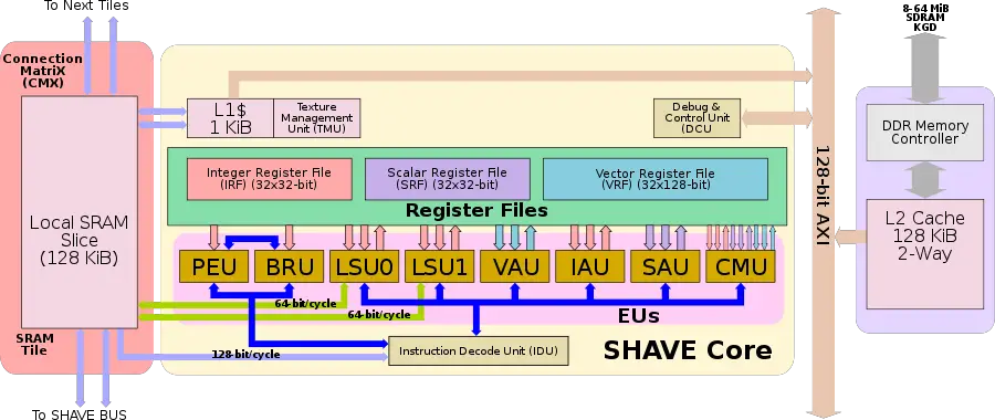
Individual Core
Overview
Architecturally, SHAVE is organized similar to IBM's CELL architecture. There are independent SHAVE cores, with up to eight in this generation may be chained together. Cores benefit from zero penalty from their two neighbors closest, an intrinsic property of architecture that inherently benefits most code. The chip features an L2 cache that is shared by all the cores as well as an integrated DDR2 memory controller that is connected to an on-package KGD stacked die ranging from 8 to 64 MiB of SDRAM.
A large set of peripherals are attached to the parameter of the chip which communicate with the cores via the AXI bus. Those peripherals include support for two high-resolution cameras (up to 12 megapixel) at high rate and high-resolution LCD controllers. The various peripherals can be software-multiplexed via the limited number of I/O pins in the package. The overall management controller core is a synthesizable SPARC V8 LEON3.
Core
The underlying concept behind the SHAVE core is extracting significant data-level parallelism. Each SHAVE core is a variable-length very long instruction word (VLLIW) processor that can operates on native 32-bit integer and 128-bit vector values. Each core incorporates a number of different types of register files as well as a large set of execution units that make use of the multiple register files with a large number of ports in order to operate on a relatively big set of values at once.
Every SHAVE core resides on an independent power island. Although we were not able to verify this, presumably you can enable and disable cores based on your power requirements through software.
Register Files
There are three register files: Integer Register File (IRF), Scalar Register File (SRF), Vector Register File (VRF).
The SHAVE's integer register file (IRF) has 17 ports in order enable a large set of parallel data operations each cycle. The IRF has 32 entries of 32-bit integers which are predominantly operated on by the IAU and the SAU. In addition to the IRF is the scalar register file (SRF) which has another set of 32 entries of 32-bit integers. The reason for the second register is to allow the SHAVE to do various three-operand operations and generate predicates for the execution units.
The SHAVE core also has a dedicated vector register file (VRF) which contains 32 entries, each 128-bit wide.
Execution Units
The three major arithmetic execution units are the vector arithmetic unit (VAU), the scalar arithmetic unit (SAU), and the integer arithmetic unit (IAU).
The integer arithmetic unit (IAU) performs all arithmetic instructions that operate on 32-bit integer numbers and access the IRF. The scalar arithmetic unit (SAU) is far more versatile and can perform all integer (8-32 bit) and floating point (HP/FP) operations. The vector arithmetic unit (VAU) supports 128-bit vector operations of all the integer (8-32 bit) and floating point (HP/FP) types.
In addition to those units, there is also a compare-move unit (CMU) which is used to generate predicates. This unit can do things such as three comparison operations per 16-bit/32-bit/8bit entry in the vector register file in parallel with the vector operations which can generate predicates for predicated execution. The CMU effectively interfaces with all the register files and is capable of moving data between them.
Bandwidth
Each of the registers files in the core incorporate a large number of ports. That, along with wide buses allow for very high sustainable throughput to be achieved at very low clock frequencies (180 MHz).
| Bandwidth | |||||||||
|---|---|---|---|---|---|---|---|---|---|
| Parameter | VRF | SRF | IRF | LSU | IDC | L1 | ISB | L2 | SDRAM |
| Clk | 180 MHz | ||||||||
| Bytes | 16 | 4 | 4 | 8 | 16 | 8 | 16 | 16 | 4 |
| Ports | 12 | 12 | 17 | 2 | 1 | 1 | 2 | 1 | 2 |
| Bandwidth | 34.56 | 8.64 | 12.24 | 2.88 | 2.88 | 1.44 | 5.76 | 2.88 | 1.44 |
| SHAVE cores | 8 | ||||||||
| Total BW | 276.48 | 69.12 | 97.92 | 23.04 | 23.04 | 11.52 | 46.08 | ||
| Total | 547.2 | 2.88 | 1.44 | ||||||
Sparse Data Acceleration
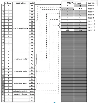
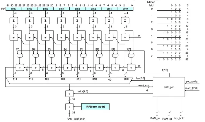
The SHAVE cores support sparse data operations with the load-store unit using eight 4-bit fields to generate the address.
Performance claims
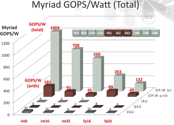
Movidius reported very high performance numbers for their chip. Fabricated on a 65 nm process and operating at 180 MHz and consuming 300 milliwatt, the full chip is capable of doing 300 GOPS or just over 1 TOPS per watt for 8-bit arithmetic for their integer arithmetic operations and 60 GOPS for 8-bit vector operations.
Package
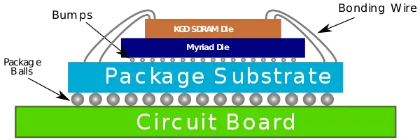
Movidius packaged those chips in an 8x8 mm BGA package with 225 balls. The die is then bumpped on top of a custom FR-4 substrate. The SDRAM is then wire bond on top of the Myriad die.
Floorplan
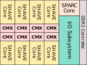
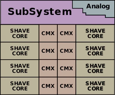
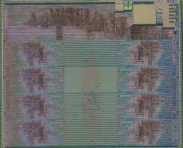
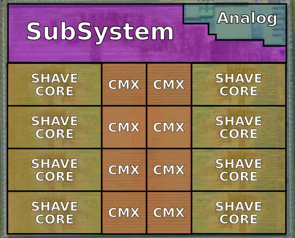
The full chip consists of just two macros - the CMX block and the SHAVE core block. The whole die was place and routed with those two marcros with the rest routed flat at the end.
Myriad Die
- TSMC's 65nm Low Power (65LP) process
- < 64 mm² die size
References
- Some information was obtained directly from Movidius
- HotChips 23 (HC23), 2011
| codename | SHAVE v2.0 + |
| designer | Movidius + |
| first launched | 2011 + |
| full page name | movidius/microarchitectures/shave v2.0 + |
| instance of | microarchitecture + |
| instruction set architecture | SHAVE + and SPARC v8 + |
| manufacturer | TSMC + |
| name | SHAVE v2.0 + |
| phase-out | 2014 + |
| process | 64 nm (0.064 μm, 6.4e-5 mm) + |
