From WikiChip
Difference between revisions of "intel/core i5/i5-1035g7"
(→Memory controller: added clarification...) |
|||
| (4 intermediate revisions by the same user not shown) | |||
| Line 25: | Line 25: | ||
|microarch=Ice Lake (Client) | |microarch=Ice Lake (Client) | ||
|platform=Ice Lake | |platform=Ice Lake | ||
| − | |core name= | + | |core name=Ice Lake U |
|core family=6 | |core family=6 | ||
|process=10 nm | |process=10 nm | ||
| Line 67: | Line 67: | ||
== Memory controller == | == Memory controller == | ||
| + | The Core i5-1035G7 has a 128-bit bus, supporting quad-channel (4x32b) LPDDR4X-3733 or dual-channel (2x64b) DDR4-3200. | ||
{{memory controller | {{memory controller | ||
|type=LPDDR4X-3733 | |type=LPDDR4X-3733 | ||
| Line 75: | Line 76: | ||
|channels=4 | |channels=4 | ||
|width=32 bit | |width=32 bit | ||
| + | |width 2=64 bit | ||
|max bandwidth=55.63 GiB/s | |max bandwidth=55.63 GiB/s | ||
|bandwidth schan=13.91 GiB/s | |bandwidth schan=13.91 GiB/s | ||
| Line 103: | Line 105: | ||
| max memory = 64 GiB | | max memory = 64 GiB | ||
| frequency = 300 MHz | | frequency = 300 MHz | ||
| − | | max frequency = 1, | + | | max frequency = 1,050 MHz |
| output crt = | | output crt = | ||
| Line 248: | Line 250: | ||
|amdpbod=No | |amdpbod=No | ||
}} | }} | ||
| + | |||
| + | == Die == | ||
| + | {{main|intel/microarchitectures/ice_lake_(client)#SoC|l1=Ice Lake SoC Die}} | ||
| + | |||
| + | :[[File:ice lake die (quad core) (annotated).png|500px|link=intel/microarchitectures/ice_lake_(client)#SoC]] | ||
| + | |||
| + | :[[File:ice lake die (quad core).png|500px|link=intel/microarchitectures/ice_lake_(client)#SoC]] | ||
Latest revision as of 08:26, 28 February 2020
| Edit Values | |
| Core i5-1035G7 | |
 | |
| General Info | |
| Designer | Intel |
| Manufacturer | Intel |
| Model Number | i5-1035G7 |
| Market | Mobile |
| Introduction | August 1, 2019 (announced) August 1, 2019 (launched) |
| Release Price | $309.00 (tray) |
| Shop | Amazon |
| General Specs | |
| Family | Core i5 |
| Series | i7-10000 |
| Locked | Yes |
| Frequency | 1,200 MHz |
| Turbo Frequency | 3,700 MHz (1 core), 3,300 MHz (4 cores) |
| Bus type | OPI |
| Bus rate | 4 × 4 GT/s |
| Clock multiplier | 12 |
| Microarchitecture | |
| ISA | x86-64 (x86) |
| Microarchitecture | Ice Lake (Client) |
| Platform | Ice Lake |
| Core Name | Ice Lake U |
| Core Family | 6 |
| Process | 10 nm |
| Technology | CMOS |
| Word Size | 64 bit |
| Cores | 4 |
| Threads | 8 |
| Max Memory | 64 GiB |
| Multiprocessing | |
| Max SMP | 1-Way (Uniprocessor) |
| Electrical | |
| TDP | 15 W |
| cTDP down | 12 W |
| cTDP down frequency | 800 MHz |
| cTDP up | 25 W |
| cTDP up frequency | 1,500 MHz |
| Packaging | |
| Package | FCBGA-1510 (BGA) |
| Contacts | 1510 |
 | |
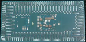
Core i5-1035G7 is a 64-bit quad-core mid-range performance x86 mobile microprocessor introduced by Intel in mid-2019. This processor, which is based on the Ice Lake microarchitecture, is manufactured on Intel's 2nd generation enhanced 10nm+ process. The i5-1035G7 operates at 1.2 GHz with a TDP of 15 W and Turbo Boost frequency of up to 3.7 GHz. This chip supports up to 64 GiB of quad-channel LPDDR4X-3733 memory and incorporates Intel's GPU with a burst frequency of 1.05 GHz.
This model supports a configurable TDP of TDP-up of 25 W.
Cache[edit]
- Main article: Ice Lake § Cache
|
Cache Organization
Cache is a hardware component containing a relatively small and extremely fast memory designed to speed up the performance of a CPU by preparing ahead of time the data it needs to read from a relatively slower medium such as main memory. The organization and amount of cache can have a large impact on the performance, power consumption, die size, and consequently cost of the IC. Cache is specified by its size, number of sets, associativity, block size, sub-block size, and fetch and write-back policies. Note: All units are in kibibytes and mebibytes. |
|||||||||||||||||||||||||||||||||||||
|
|||||||||||||||||||||||||||||||||||||
Memory controller[edit]
The Core i5-1035G7 has a 128-bit bus, supporting quad-channel (4x32b) LPDDR4X-3733 or dual-channel (2x64b) DDR4-3200.
|
Integrated Memory Controller
|
||||||||||||||||
|
||||||||||||||||
Expansions[edit]
Expansion Options |
|||||
|
|||||
Graphics[edit]
|
Integrated Graphics Information
|
|||||||||||||||||||||||||||||||||||||||||||||||||||||||||||||||||
|
|||||||||||||||||||||||||||||||||||||||||||||||||||||||||||||||||
Features[edit]
[Edit/Modify Supported Features]
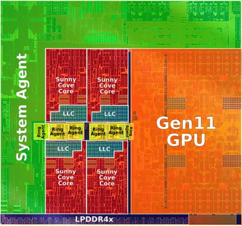
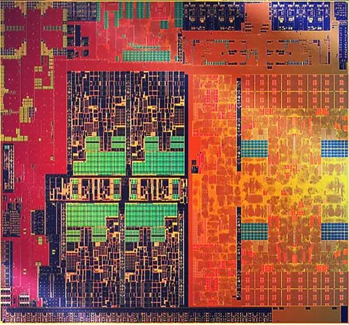
Die[edit]
- Main article: Ice Lake SoC Die
Facts about "Core i5-1035G7 - Intel"
| back image |  + + |
| base frequency | 1,200 MHz (1.2 GHz, 1,200,000 kHz) + |
| bus links | 4 + |
| bus rate | 4,000 MT/s (4 GT/s, 4,000,000 kT/s) + |
| bus type | OPI + |
| clock multiplier | 12 + |
| core count | 4 + |
| core family | 6 + |
| core name | Ice Lake U + |
| designer | Intel + |
| device id | 0x8A52 + |
| family | Core i5 + |
| first announced | August 1, 2019 + |
| first launched | August 1, 2019 + |
| full page name | intel/core i5/i5-1035g7 + |
| has advanced vector extensions | true + |
| has advanced vector extensions 2 | true + |
| has advanced vector extensions 512 | true + |
| has ecc memory support | false + |
| has extended page tables support | true + |
| has feature | Advanced Vector Extensions +, Advanced Vector Extensions 2 +, Advanced Vector Extensions 512 +, Advanced Encryption Standard Instruction Set Extension +, Hyper-Threading Technology +, Turbo Boost Technology 2.0 +, Enhanced SpeedStep Technology +, Speed Shift Technology +, Intel VT-x +, Intel VT-d +, Extended Page Tables +, Memory Protection Extensions +, Software Guard Extensions +, Secure Key Technology +, OS Guard + and Flex Memory Access + |
| has intel enhanced speedstep technology | true + |
| has intel flex memory access support | true + |
| has intel secure key technology | true + |
| has intel speed shift technology | true + |
| has intel supervisor mode execution protection | true + |
| has intel turbo boost technology 2 0 | true + |
| has intel vt-d technology | true + |
| has intel vt-x technology | true + |
| has locked clock multiplier | true + |
| has second level address translation support | true + |
| has simultaneous multithreading | true + |
| has x86 advanced encryption standard instruction set extension | true + |
| instance of | microprocessor + |
| integrated gpu | Iris Plus Graphics + |
| integrated gpu base frequency | 300 MHz (0.3 GHz, 300,000 KHz) + |
| integrated gpu designer | Intel + |
| integrated gpu execution units | 64 + |
| integrated gpu max frequency | 1,050 MHz (1.05 GHz, 1,050,000 KHz) + |
| integrated gpu max memory | 65,536 MiB (67,108,864 KiB, 68,719,476,736 B, 64 GiB) + |
| isa | x86-64 + |
| isa family | x86 + |
| l1$ size | 320 KiB (327,680 B, 0.313 MiB) + |
| l1d$ description | 12-way set associative + |
| l1d$ size | 192 KiB (196,608 B, 0.188 MiB) + |
| l1i$ description | 8-way set associative + |
| l1i$ size | 128 KiB (131,072 B, 0.125 MiB) + |
| l2$ description | 8-way set associative + |
| l2$ size | 2 MiB (2,048 KiB, 2,097,152 B, 0.00195 GiB) + |
| l3$ description | 12-way set associative + |
| l3$ size | 6 MiB (6,144 KiB, 6,291,456 B, 0.00586 GiB) + |
| ldate | August 1, 2019 + |
| main image |  + + |
| manufacturer | Intel + |
| market segment | Mobile + |
| max cpu count | 1 + |
| max memory | 65,536 MiB (67,108,864 KiB, 68,719,476,736 B, 64 GiB, 0.0625 TiB) + |
| max memory bandwidth | 55.63 GiB/s (56,965.12 MiB/s, 59.732 GB/s, 59,732.258 MB/s, 0.0543 TiB/s, 0.0597 TB/s) + |
| max memory channels | 4 + |
| max usb ports | 4 + |
| microarchitecture | Ice Lake (Client) + |
| model number | i5-1035G7 + |
| name | Core i5-1035G7 + |
| package | FCBGA-1510 + |
| platform | Ice Lake + |
| process | 10 nm (0.01 μm, 1.0e-5 mm) + |
| release price | $ 309.00 (€ 278.10, £ 250.29, ¥ 31,928.97) + |
| release price (tray) | $ 309.00 (€ 278.10, £ 250.29, ¥ 31,928.97) + |
| series | i7-10000 + |
| smp max ways | 1 + |
| supported memory type | LPDDR4X-3733 + and DDR4-3200 + |
| tdp | 15 W (15,000 mW, 0.0201 hp, 0.015 kW) + |
| tdp down | 12 W (12,000 mW, 0.0161 hp, 0.012 kW) + |
| tdp down frequency | 800 MHz (0.8 GHz, 800,000 kHz) + |
| tdp up | 25 W (25,000 mW, 0.0335 hp, 0.025 kW) + |
| tdp up frequency | 1,500 MHz (1.5 GHz, 1,500,000 kHz) + |
| technology | CMOS + |
| thread count | 8 + |
| turbo frequency (1 core) | 3,700 MHz (3.7 GHz, 3,700,000 kHz) + |
| turbo frequency (4 cores) | 3,300 MHz (3.3 GHz, 3,300,000 kHz) + |
| word size | 64 bit (8 octets, 16 nibbles) + |
| x86/has memory protection extensions | true + |
| x86/has software guard extensions | true + |

