(→Key changes from {{\\|ARM3}}) |
(→Block Diagram) |
||
| Line 62: | Line 62: | ||
=== Block Diagram === | === Block Diagram === | ||
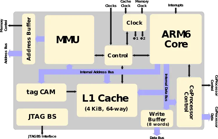
==== Entire Chip (610) ==== | ==== Entire Chip (610) ==== | ||
| − | : [[File: | + | : [[File:arm610 block diagram.svg|750px]] |
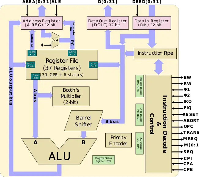
==== Core ==== | ==== Core ==== | ||
| − | + | : [[File:arm6 block diagram.svg|650px]] | |
=== Memory Hierarchy === | === Memory Hierarchy === | ||
Revision as of 23:02, 9 September 2017
| Edit Values | |
| ARM6 µarch | |
| General Info | |
| Arch Type | CPU |
| Designer | ARM Holdings |
| Manufacturer | VLSI Technology, GEC-Plessey Semiconductors, Sharp |
| Introduction | 1993 |
| Process | 0.8 µm |
| Core Configs | 1 |
| Pipeline | |
| Type | Scalar, Pipelined |
| Stages | 3 |
| Decode | 1-way |
| Instructions | |
| ISA | ARMv3 |
| Cache | |
| L1 Cache | 4 KiB/core 64-way set associative |
| Succession | |
ARM6 is an ARM microarchitecture designed by ARM Holdings and introduced in 1993 as a successor to the ARM3. This was the first design by ARM as an independent company after being spun-off from Acorn Computers.
Contents
History
- See also: ARM's History
Following ARM's incorporation in November 1990 after being spun-off from Acorn Computers, ARM continued to develop the ARM microprocessor. In 1993 ARM introduced the ARM6 MacroCell, a substantial improvement over the previous ARM3 microarchitecture. The same year ARM signed with a number of additional licensees beyond VLSI Technology, including Sharp and GEC-Plessey.
The popularity of the ARM6 can be largely attributed to Apple's adaptation of the processor in their Newton PDAs.
Process Technology
- See also: 0.8 µm process
The ARM6 was implemented on a 0.8 µm CMOS process.
Architecture
The ARM6 microarchitecture (MacroCell) was used for the ARM60, ARM600, and the ARM610. The ARM250 borrowed much of the architecture but used an ARM3 core instead. The various ARM6 improvements were heavily influenced directly by Apple's needs from their Newton PDA project.
Key changes from ARM3
- 32-bit address space (from 26-bit)
- Can map 4 GiB of memory
- CPSR & SPSR moved out of the program counter
- Their own separate registers
- New Modes
- Abort (abt)
- Undefined (und)
- Virtual memory
- Integrated MMU
- Write Buffer
- Testability
- JTAG Boundary Scan Interface
New instructions
New ARM6 instructions:
Movement:
-
MRS- Move from register to CPSR/SPSR -
MSR- Move from CPSR/SPSR to register
Block Diagram
Entire Chip (610)
Core
Memory Hierarchy
- Cache
- L1 Cache (unified)
- 4 KiB, 64-way set associative
- 16 B line size
- Write-through policy
- Per core
- L1 Cache (unified)
- System DRAM
- Up to 4 GiB
- TLB
- 32 entries
- 4 KiB small pages, 1 KiB sub pages
- 64 KiB large pages, 16 KiB sub pages
Overview
- See also: ARMv3
The ARM6 is a further evolutionary enhancement of the ARM3. The new chip integrated a number of highly desired features - particularly ones needed by Apple. The ARM6, departs from all the previous ARM chips by featuring a full 32-bit address and data buses. To facilitate the larger address space, ARM (previously Acorn) had to move the status flags from the program counter to its own independent register. In total, the ARM6 has 37 registers consisting of 31 32-bit general-purpose registers and 6 additional status registers.
Pipeline
- Main article: ARM2 Pipeline
ARM6's pipeline is identical to the ARM2.
Cache
For the most part, the ARM6's Instruction and Data Cache (IDC) is identical to the ARM3 implementation. The IDC consists of 256 lines of 4 words each (i.e., 16 B) organized as 4 blocks of 64 lines for a 64-way set associative. The IDC operates on virtual addresses generated by the ARM6 core. Memory reads are done on whole lines.
The IDC is disabled on RESET and may be programmatically disabled or enabled via a control register. The Memory Management Page Tables also provide two bits for marking operation modes - Cacheable and Updateable. The Cacheable bit is used to specify if a certain address may be cached or not. For example, operations that require pulling I/O data need to be able to do so directly without retrieving invalidated data from the cache. The Updateable is further used to indicate that a memory write should immediately update with external memory to maintain consistency.
The ARM610 also incorporates a write buffer for additional performance. The buffer can store up to eight words and up to two addresses. As with the IDC, the write buffer may be enabled or disabled and is controlled via a Bufferable bit which can set whether a certain address space is bufferable allowing main memory to be buffered while I/O space to be unbuffered.
Memory Management Unit
By far the biggest addition to the ARM6 is the addition of an MMU which is in charge of translating virtual addresses into physical ones as well as control access permissions. The MMU is implemented using a 32-entry Translation Lookaside Buffer (TLB), access control logic, and translation table walking logic.
The MMU operates on sections comprised of 1 MiB blocks. Two page sizes are supported: 4 KiB small pages and 64 KiB large pages. Both taking up a single entry in the TLB. Each of the pages has a more granular access control which extend to 1 KiB sub-pages (on the small pages) and 16 KiB sub-pages (on the large pages). Upon a hit in the TLB, control logic is used to determine if the access is permitted. On denial, the MMU signals the core to abort. On a miss, the translation table walking logic is used to retrieve the translation information from a full translation table in physical memory. Entries are replaced cyclically.
When the MMU is disabled, such as during RESET, the virtual address is the physical address. Note that because the MMU stores the cache control bits (i.e., Cacheable, Updateable), for the chip to use the IDC, the MMU must also be enabled.
Four types of faults can be generated on the ARM6: Alignment Fault, Translation Fault, Domain Fault, Permission Fault. If the fault is a result of a memory access, the access is aborted and the appropriate signals are sent to the core. The core recognizes two abort types: data abort and prefetch abort which are handled separately by the MMU.
Die
ARM6 MacroCell
- 3.1 mm x 1.9 mm
- 5.89 mm² die size
- 54 mW @ 20 MHz @ 3 Volt
- 0.8 µm CMOS
- 35,530 transistors
ARM610
- 26.45 mm² die size
- 358,931 transistors
- TQFP-144
The ARM610 fabricated by GEC-Plessey, on a 0.8 µm process, reported to be 8.87 mm x 8.67 for a total die size of 76.9 mm².
All ARM6 Chips
| List of ARM6-based Processors | ||||||||||||
|---|---|---|---|---|---|---|---|---|---|---|---|---|
| Model | Manufacturer | Core | Launched | Frequency | Power Dissipation | Max Memory | ||||||
| VY86C060 | VLSI Technology | ARM60 | 1993 | 20 MHz 0.02 GHz , 25 MHz20,000 kHz 0.025 GHz 25,000 kHz | 4 GiB 4,096 MiB 4,194,304 KiB 4,294,967,296 B 0.00391 TiB | |||||||
| VY86C06020 | VLSI Technology | ARM60 | 1994 | 20 MHz 0.02 GHz 20,000 kHz | 4 GiB 4,096 MiB 4,194,304 KiB 4,294,967,296 B 0.00391 TiB | |||||||
| VY86C06040 | VLSI Technology | ARM60 | 1994 | 40 MHz 0.04 GHz 40,000 kHz | 4 GiB 4,096 MiB 4,194,304 KiB 4,294,967,296 B 0.00391 TiB | |||||||
| VY86C060A | VLSI Technology | ARM60 | 1994 | 33 MHz 0.033 GHz 33,000 kHz | 4 GiB 4,096 MiB 4,194,304 KiB 4,294,967,296 B 0.00391 TiB | |||||||
| VY86C061 | VLSI Technology | ARM60 | 1993 | 20 MHz 0.02 GHz , 25 MHz20,000 kHz 0.025 GHz 25,000 kHz | 4 GiB 4,096 MiB 4,194,304 KiB 4,294,967,296 B 0.00391 TiB | |||||||
| VY86C610 | VLSI Technology | ARM610 | 1993 | 20 MHz 0.02 GHz , 25 MHz20,000 kHz 0.025 GHz 25,000 kHz | 4 GiB 4,096 MiB 4,194,304 KiB 4,294,967,296 B 0.00391 TiB | |||||||
| VY86C610C | VLSI Technology | ARM610 | 23 July 1994 | 33 MHz 0.033 GHz 33,000 kHz | 0.5 W 500 mW 6.705e-4 hp 5.0e-4 kW | 4 GiB 4,096 MiB 4,194,304 KiB 4,294,967,296 B 0.00391 TiB | ||||||
| Count: 7 | ||||||||||||
References
- Muller, Mike. "ARM6: a high performance low power consumption macrocell." Compcon Spring'93, Digest of Papers.. IEEE, 1993.
- Licensees, Welcomes New. "ARM Semiconductor Welcomes New Licensees." Microelectronics Journal 24.7 (1993): 7.
| codename | ARM6 + |
| core count | 1 + |
| designer | ARM Holdings + |
| first launched | 1993 + |
| full page name | arm holdings/microarchitectures/arm6 + |
| instance of | microarchitecture + |
| instruction set architecture | ARMv3 + |
| manufacturer | VLSI Technology +, GEC-Plessey Semiconductors + and Sharp + |
| microarchitecture type | CPU + |
| name | ARM6 + |
| pipeline stages | 3 + |
| process | 800 nm (0.8 μm, 8.0e-4 mm) + |

