Semiconductor & Computer Engineering
From WikiChip
Lake Crest - Microarchitectures - Intel Nervana
| Edit Values | |
| Lake Crest µarch | |
| General Info | |
| Arch Type | NPU |
| Designer | Nervana |
| Manufacturer | TSMC |
| Introduction | November 17, 2016 |
| Process | 28 nm |
| Succession | |
Lake Crest is a neural processor microarchitecture designed by Nervana.
Contents
Process Technology
Lake Crest is fabricated on TSMC's 28 nm process.
Architecture
Lake Crest was designed from the ground up for deep learning. The architecture itself is a tensor-based architecture, meaning it's optimized for blocks of compute instead of operating on scalars (as would a traditional Intel CPU would).
- Tensor-based architecture
- Nervana Engine
- Flexpoint number format
- No caches
- Software explicitly manages all on-chip memory
- HBM2 memory
- 32 GiB of in-package memory
- 8 Tbit/s bandwidth
- 12 x Inter-Chip Links (ICL)
- bi-directional high-bandwidth direct chip-to-chip interconnect
- 100 GB/s (1,200 GB/s aggregate)
This list is incomplete; you can help by expanding it.
Block Diagram
Chip

Processing Cluster
| This section is empty; you can help add the missing info by editing this page. |
Memory Hierarchy
- 32 GiB on-package HBM2
- 1 TiB/s
Die
Nervana stated that Lake Crest is "near-reticle size" implying the die size is likely around the 650-750 mm².
- TSMC 28 nm process
- 650-750 mm² die size
Additional Shots
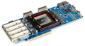
Lake Crest Accelerator PCIe card (internal view)

Bibliography
- Rao, N. (2016, November). Pathfinding and Hardware Deep Dive. 2016 AI Day, San Francisco.
- Rao, N. (2018, May). Keynote presentation. 2018 AI DevCon, San Francisco.
Facts about "Lake Crest - Microarchitectures - Intel Nervana"
| codename | Lake Crest + |
| designer | Nervana + |
| first launched | November 17, 2016 + |
| full page name | nervana/microarchitectures/lake crest + |
| instance of | microarchitecture + |
| manufacturer | TSMC + |
| name | Lake Crest + |
| process | 28 nm (0.028 μm, 2.8e-5 mm) + |