Semiconductor & Computer Engineering
From WikiChip
Difference between revisions of "nervana/microarchitectures/lake crest"
m (Reverted edits by 174.117.140.200 (talk) to last revision by David) |
|||
| (13 intermediate revisions by 4 users not shown) | |||
| Line 5: | Line 5: | ||
|designer=Nervana | |designer=Nervana | ||
|manufacturer=TSMC | |manufacturer=TSMC | ||
| + | |introduction=November 17, 2016 | ||
|process=28 nm | |process=28 nm | ||
| − | |successor= | + | |successor=Spring Crest |
|successor link=nervana/microarchitectures/spring crest | |successor link=nervana/microarchitectures/spring crest | ||
}} | }} | ||
'''Lake Crest''' is a [[neural processor]] microarchitecture designed by [[Nervana]]. | '''Lake Crest''' is a [[neural processor]] microarchitecture designed by [[Nervana]]. | ||
| + | |||
| + | == Process Technology == | ||
| + | Lake Crest is fabricated on [[TSMC]]'s [[28 nm process]]. | ||
| + | |||
| + | == Architecture == | ||
| + | Lake Crest was designed from the ground up for [[deep learning]]. The architecture itself is a tensor-based architecture, meaning it's optimized for blocks of compute instead of operating on scalars (as would a traditional Intel CPU would). | ||
| + | * Tensor-based architecture | ||
| + | ** Nervana Engine | ||
| + | * [[Flexpoint]] number format | ||
| + | * No caches | ||
| + | ** Software explicitly manages all on-chip memory | ||
| + | * HBM2 memory | ||
| + | ** 32 GiB of in-package memory | ||
| + | ** 8 Tbit/s bandwidth | ||
| + | * 12 x Inter-Chip Links (ICL) | ||
| + | ** bi-directional high-bandwidth direct chip-to-chip interconnect | ||
| + | ** 100 GB/s (1,200 GB/s aggregate) | ||
| + | |||
| + | {{expand list}} | ||
| + | |||
| + | === Block Diagram === | ||
| + | ==== Chip ==== | ||
| + | :[[File:knights crest chip block diagram.svg|700px]] | ||
| + | ==== Processing Cluster ==== | ||
| + | {{empty section}} | ||
| + | |||
| + | === Memory Hierarchy === | ||
| + | * 32 GiB on-package [[HBM2]] | ||
| + | ** 1 TiB/s | ||
| + | |||
| + | == Die == | ||
| + | Nervana stated that Lake Crest is "near-reticle size" implying the die size is likely around the 650-750 mm². | ||
| + | |||
| + | * TSMC [[28 nm process]] | ||
| + | * 650-750 mm² die size | ||
| + | |||
| + | == Additional Shots == | ||
| + | <gallery mode=slideshow> | ||
| + | File:lake crest pcie card internal.png|Lake Crest Accelerator PCIe card (internal view) | ||
| + | </gallery> | ||
| + | |||
| + | == Bibliography == | ||
| + | * Rao, N. (2016, November). ''Pathfinding and Hardware Deep Dive''. 2016 AI Day, San Francisco. | ||
| + | * Rao, N. (2018, May). ''Keynote presentation''. 2018 AI DevCon, San Francisco. | ||
Latest revision as of 16:51, 6 August 2020
| Edit Values | |
| Lake Crest µarch | |
| General Info | |
| Arch Type | NPU |
| Designer | Nervana |
| Manufacturer | TSMC |
| Introduction | November 17, 2016 |
| Process | 28 nm |
| Succession | |
Lake Crest is a neural processor microarchitecture designed by Nervana.
Contents
Process Technology[edit]
Lake Crest is fabricated on TSMC's 28 nm process.
Architecture[edit]
Lake Crest was designed from the ground up for deep learning. The architecture itself is a tensor-based architecture, meaning it's optimized for blocks of compute instead of operating on scalars (as would a traditional Intel CPU would).
- Tensor-based architecture
- Nervana Engine
- Flexpoint number format
- No caches
- Software explicitly manages all on-chip memory
- HBM2 memory
- 32 GiB of in-package memory
- 8 Tbit/s bandwidth
- 12 x Inter-Chip Links (ICL)
- bi-directional high-bandwidth direct chip-to-chip interconnect
- 100 GB/s (1,200 GB/s aggregate)
This list is incomplete; you can help by expanding it.
Block Diagram[edit]
Chip[edit]

Processing Cluster[edit]
| This section is empty; you can help add the missing info by editing this page. |
Memory Hierarchy[edit]
- 32 GiB on-package HBM2
- 1 TiB/s
Die[edit]
Nervana stated that Lake Crest is "near-reticle size" implying the die size is likely around the 650-750 mm².
- TSMC 28 nm process
- 650-750 mm² die size
Additional Shots[edit]
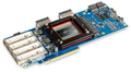
Lake Crest Accelerator PCIe card (internal view)

Bibliography[edit]
- Rao, N. (2016, November). Pathfinding and Hardware Deep Dive. 2016 AI Day, San Francisco.
- Rao, N. (2018, May). Keynote presentation. 2018 AI DevCon, San Francisco.
Facts about "Lake Crest - Microarchitectures - Intel Nervana"
| codename | Lake Crest + |
| designer | Nervana + |
| first launched | November 17, 2016 + |
| full page name | nervana/microarchitectures/lake crest + |
| instance of | microarchitecture + |
| manufacturer | TSMC + |
| name | Lake Crest + |
| process | 28 nm (0.028 μm, 2.8e-5 mm) + |