| Edit Values | |
| Socket F | |
| General Info | |
| Designer | AMD |
| Introduction | August 15, 2006 (launched) |
| Market | Server |
| Microarchitecture | K8, K10 |
| TDP | 137 W 137,000 mW 0.184 hp 0.137 kW |
| Package | |
| Name | LGA-1207 |
| Type | Organic Flip-Chip Land Grid Array |
| Contacts | 1207 |
| Dimension | 40.00 mm 4 cm × 40.00 mm1.575 in 4 cm 1.575 in |
| Pitch | 1.10 mm 0.0433 in |
| Socket | |
| Name | Socket F |
| Type | LGA |
Socket F was AMD's second socket for server platforms, a socket for LGA-1207-packaged AMD Opteron and Athlon 64 FX microprocessors with integrated DDR2 memory controllers. It succeeded Socket 940 which has a DDR interface and like Socket F supports three HyperTransport links to connect the processors in 2-, 4-, and 8-socket systems. Uniprocessor Opterons with a DDR2 interface were released in packages for Socket AM2 and AM2+ with a single HT link. Socket F was superseded by Socket C32 and G34 which support DDR3 memory.
AMD developed five revisions of Socket F:
- The initial Socket F a.k.a. Fr1 was designed for Opteron "Santa Rosa" processors which are members of AMD's NPT Family 0Fh with dual CPU cores based on the K8 microarchitecture and fabricated on a 90 nm process. Its desktop counterpart is Socket AM2. This socket is compatible with Fr1, Fr2, and Fr5 package processors.
- Socket Fr2 (August 2007) is an improved version for Family 10h processors with four CPU cores based on the K10 microarchitecture and fabricated on a 65 nm process. It raised the maximum memory data rate to 800 MT/s and uses dual power planes supplying the cores and northbridge, a power saving feature. Its desktop counterpart is Socket AM2+. Socket Fr2 is compatible with Fr1, Fr2, Fr5, and Fr6 package processors.
- Socket Fr3 a.k.a. 1207 FX or Socket L1 (November 2006) was derived from Fr1 for dual-core Athlon 64 FX processors on the dual-socket Quad FX a.k.a. "4x4" desktop platform. These processors support UDIMMs instead of RDIMMs. Socket Fr3 is incompatible with packages for other revisions.
- Socket Fr5 (November 2008) is an improved version for Family 10h rev. C and later processors fabricated on a 45 nm process. It supports HyperTransport Gen 3 on inter-socket links. Socket Fr5 is compatible with Fr1, Fr2, Fr5, and Fr6 package processors.
- Socket Fr6 (June 2009) accommodates Opteron "Istanbul" processors with six cores and 6 MiB L3 cache. It supports HyperTransport Gen 3 on I/O and inter-socket links, AMD's HT Assist (probe filter) technology, APML, and raises the maximum HT data rate to 4800 MT/s. This socket is compatible with Fr5 and Fr6 packages. Fr5 packages in Socket Fr6 support HT Gen 3 on all links.
The memory controllers of Family 10h can be configured for DDR2 and DDR3 DIMMs. Opteron DP and MP models with a DDR3 interface were released in a LGA-1207 package for Socket C32 and a LGA-1944 package for Socket G34. The packages for Socket F and C32 have the same dimensions but are mechanically, due to keying notches in different positions, and presumably electrically, incompatible with the opposite socket. Uniprocessor Opterons with a DDR3 interface use Socket AM3 and AM3+.
All three HyperTransport links on Socket F support connections to I/O devices. On dual-processor models any one of these links may connect to another DP or MP processor. On multiprocessor models all three links support cache coherent connections to other DP or MP processors.
Contents
Features
- 1207-land lidded land grid array package, 40 × 40 mm, 35 × 35 land array, 1.1 mm pitch, organic substrate, C4 (flip chip) die attachment
- 2 × 64/72 bit DDR2 SDRAM interface up to 333 MHz, PC2-5300 (DDR2-667), 10.7 GB/s (Fr1)
- 2 × 64/72 bit DDR2 SDRAM interface up to 400 MHz, PC2-6400 (DDR2-800), 12.8 GB/s (Fr2, Fr5, Fr6)
- Up to 8 RDIMMs (Fr1, Fr2, Fr5, Fr6), up to 4 UDIMMs (Fr3)
- JEDEC SSTL_1.8
- SEC-DED ECC support
- On-line spare feature provides single-rank DRAM redundancy
- 3 × 16 bit HyperTransport 1.0 interface up to 1000 MHz, 2000 MT/s, 4.0 GB/s in each direction (Fr1, Fr2, Fr3)
- 3 × 16 bit HyperTransport 1.0/3.0 interface up to 2200 MHz, 4400 MT/s, 8.8 GB/s in each direction (Fr5)
- 3 × 16 bit HyperTransport 1.0/3.0 interface up to 2400 MHz, 4800 MT/s, 9.6 GB/s in each direction (Fr6)
- Socket Fr5 supports only HT Gen 1 at up to 2000 MT/s on I/O links
- Managemement Features
- Advanced Platform Management Link (APML) (Fr6)
- SMBus v2.0-compatible interface
- Remote-Management Interface (SB-RMI)
- Power Management
- Multiple low-power states
- Independent Dynamic Core Technology (Fam. 10h)
- AMD CoolCore Technology (Fam. 10h)
- Dual Dynamic Power Management (dual power planes, Fam. 10h)
- ACPI-compliant
- Supported power states Fam. 10h: C0, C1, S0, S1, S3, S4, S5
Chipsets
Processors using Socket F
The Opteron 2000 series supports dual socket systems, the 8000 series are multiprocessors for systems with up to eight sockets. (Series 1000 and 3000 are uniprocessors using Socket AM2/AM2+/AM3/AM3+ instead. Series 4000 and 6000 use Socket C32 and G34, respectively, in systems with up to four sockets.)
- Opteron 2200/8200 "Santa Rosa"
- Opteron 2300/8300 "Barcelona", "Shanghai"
- Opteron 2400/8400 "Istanbul"
- Embedded Opteron (same silicon as "Barcelona" and "Istanbul")
- Athlon 64 FX dual-core "Windsor"
| List of all Socket F-based Processors | |||||||||||||||||||
|---|---|---|---|---|---|---|---|---|---|---|---|---|---|---|---|---|---|---|---|
| Model | Price | Process | Launched | µarch | Family | Core | C | T | Freq | Turbo | TDP | ||||||||
| Count: 0 | |||||||||||||||||||
Package Diagram
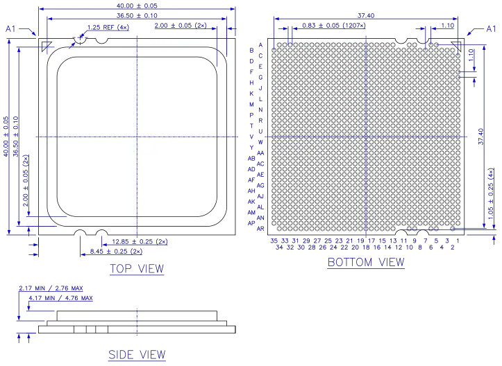
LGA-1207 Socket F package. All dimensions in millimeters.
Socket Diagram
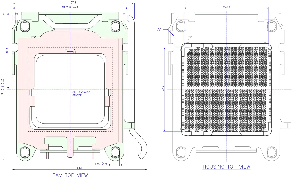
Dimensions of Foxconn Socket F (1207), Part No. PE120723-3741-01F. All dimensions in millimeters.
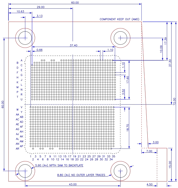
Socket F PCB layout with maximum socket outline as specified in AMD Publ. #31700. All dimensions in millimeters.
Pin Map
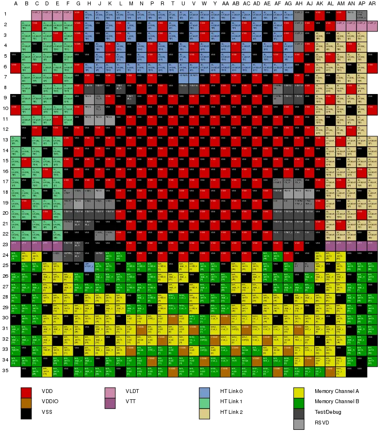
Socket Fr1 pins, package bottom view.
Pin Description
| Signal | Description |
|---|---|
| CLKIN_H/L | 200-MHz PLL Reference Clock |
| CPU_PRESENT_L | Processor is present in this socket. Shorted to VSS on the package. |
| DBRDY | Debug Ready |
| DBREQ_L | Debug Request |
| HTREF0, HTREF1 | HyperTransport Compensation Resistor to VSS, VLDT |
| LDTSTOP_L | HT Stop Control Input for power management and link width and frequency change |
| L[2:0]_CADIN_H/L[15:0] | HT Link Differential Command/Address/Data Input |
| L[2:0]_CADOUT_H/L[15:0] | HT Link Differential Command/Address/Data Output |
| L[2:0]_CLKIN_H/L[1:0] | HT Link Differential Clock Input |
| L[2:0]_CLKOUT_H/L[1:0] | HT Link Differential Clock Output |
| L[2:0]_CTLIN_H/L[1:0] | HT Link Differential Control Input |
| L[2:0]_CTLOUT_H/L[1:0] | HT Link Differential Control Output |
| MA/MB_ADD[15:0] | DRAM Column/Row Address |
| MA/MB_BANK[2:0] | DRAM Bank Address |
| MA/MB_CAS_L | DRAM Column Address Strobe |
| MA/MB_CHECK[7:0] | DRAM ECC Bits |
| MA/MB_CKE[1:0] | DRAM Clock Enable |
| MA/MB_DATA[63:0] | DRAM Data Bus |
| MA/MB_DQS_H/L[16:0] | DRAM Differential Data Strobe |
| MA/MB_ERR_L | DRAM Parity Error |
| MA/MB_PAR | DRAM Address and Control Bus Parity |
| MA/MB_RAS_L | DRAM Row Address Strobe |
| MA/MB_RESET_L | DRAM Reset pin for Suspend-to-RAM power management mode |
| MA/MB_WE_L | DRAM Write Enable |
| MA[3:0]/MB[3:0]_CLK_H/L | DRAM Differential Clock |
| MA[3:0]/MB[3:0]_CS_L[1:0] | DRAM Chip Select |
| MA[3:0]/MB[3:0]_ODT[0] | DRAM Enable Pin for On Die Termination |
| M_VREF | DRAM Interface Voltage Reference |
| M_ZN | Compensation Resistor to VSS |
| M_ZP | Compensation Resistor to VDDIO |
| PROCHOT_L | Processor in HTC-active state, open drain |
| PWROK | Voltages and CLKIN have reached specified operation |
| RESET_L | Processor Reset |
| RSVD | Reserved |
| SIC | Sideband Temperature Sensor Interface Clock |
| SID | Sideband Temperature Sensor Interface Data, open drain |
| TCK | JTAG Clock |
| TDI | JTAG Data Input |
| TDO | JTAG Data Output |
| TEST* | Test signal |
| THERMDA, THERMDC | Thermal Diode Anode, Cathode |
| THERMTRIP_L | Thermal Sensor Trip output, open drain |
| TMS | JTAG Mode Select |
| TRST_L | JTAG Reset |
| VDDA | Filtered PLL supply voltage |
| VDDIO_FB_H/L | Differential feedback to VDDIO regulator |
| VDDIO | DRAM I/O ring power supply |
| VDD_FB_H/L | Differential feedback to VDD regulator |
| VDD | Core power supply |
| VID[5:0] | Voltage ID to VDD regulator |
| VLDT_[2:0] | HyperTransport I/O ring power supply |
| VSS | Ground |
| VTT_SENSE | VTT monitor pin |
| VTT | VTT power supply |
References
- "Socket F (1207) Design Specification", AMD Publ. #31700, Rev. 1.04, July 2010
- "Thermal Design Guide for Socket F (1207) Processors", AMD Publ. #32800, Rev. 3.00, August 7, 2006
- "Socket F (1207) Processor Functional Data Sheet", AMD Publ. #31118, Rev. 1.03, March 2007
- "AMD Opteron™ Processor Product Data Sheet", AMD Publ. #23932, Rev. 3.23, March 23, 2007
- "Family 10h AMD Opteron Processor Product Data Sheet", AMD Publ. #40036, Rev. 3.04, June 22, 2010
- "BIOS and Kernel Developer's Guide for AMD NPT Family 0Fh Processors", AMD Publ. #32559, Rev. 3.16, October 31, 2009
- "BIOS and Kernel Developer’s Guide (BKDG) For AMD Family 10h Processors", AMD Publ. #31116, Rev. 3.62, January 14, 2013
- "Revision Guide for AMD NPT Family 0Fh Processors", AMD Publ. #33610, Rev. 3.48, December 13, 2011
- "Revision Guide for AMD Family 10h Processors", AMD Publ. #41322, Rev. 3.92, March 2012
See also
| designer | AMD + |
| first launched | August 15, 2006 + |
| instance of | package + |
| market segment | Server + |
| microarchitecture | K8 + and K10 + |
| name | Socket F + |
| package | LGA-1207 + |
| package contacts | 1,207 + |
| package length | 40 mm (4 cm, 1.575 in) + |
| package pitch | 1.1 mm (0.0433 in) + |
| package type | Organic Flip-Chip Land Grid Array + |
| package width | 40 mm (4 cm, 1.575 in) + |
| socket | Socket F + |
| tdp | 137 W (137,000 mW, 0.184 hp, 0.137 kW) + |


