| Edit Values | |
| Snapdragon 855 | |
 | |
| General Info | |
| Designer | Qualcomm, ARM Holdings |
| Manufacturer | TSMC |
| Model Number | SDM855 |
| Part Number | SM8150 |
| Market | Mobile |
| Introduction | December 4, 2018 (announced) Q1, 2019 (launched) |
| General Specs | |
| Family | Snapdragon 800 |
| Series | 800 |
| Frequency | 1,800 MHz, 2,420 MHz, 2,840 MHz |
| Microarchitecture | |
| ISA | ARMv8 (ARM) |
| Microarchitecture | Cortex-A76, Cortex-A55 |
| Core Name | Kryo 485 Gold, Kryo 485 Silver |
| Process | 7 nm |
| Technology | CMOS |
| Die | 73.27 mm² 8.48 mm × 8.64 mm |
| Word Size | 64 bit |
| Cores | 8 |
| Threads | 8 |
| Max Memory | 16 GiB |
| Multiprocessing | |
| Max SMP | 1-Way (Uniprocessor) |
| Packaging | |
 | |
| Succession | |
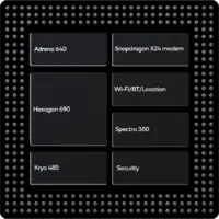
Snapdragon 855 is a high-performance 64-bit ARM LTE system on a chip designed by Qualcomm and introduced in late 2018. Fabricated on TSMC's 7nm process, the 855 features four Kryo 485 Silver high-efficiency cores operating at 1.8 GHz along with three high-performance Kryo 485 Gold operating at 2.42 GHz and another higher-performance Kryo 485 Gold core operating at 2.84 GHz. The Snapdragon 855 integrates the Adreno 640 GPU operation at ? MHz and features an X24 LTE modem supporting Cat 20 uplink and Cat 20 downlink. This chip supports up to 16 GiB of quad-channel LPDDR4X-4266 memory.
The Snapdragon 855 can be paired with Qualcomm's X50 5G modem (an external chip) and an RF front-end interface chip (RFFE) to bring 5G NR, sub-6 GHz and mmWave, support.
Contents
Cache
- Main articles: Cortex-A76 § Cache and Cortex-A55 § Cache
1+3 core cluster Cortex-A76:
|
Cache Organization
Cache is a hardware component containing a relatively small and extremely fast memory designed to speed up the performance of a CPU by preparing ahead of time the data it needs to read from a relatively slower medium such as main memory. The organization and amount of cache can have a large impact on the performance, power consumption, die size, and consequently cost of the IC. Cache is specified by its size, number of sets, associativity, block size, sub-block size, and fetch and write-back policies. Note: All units are in kibibytes and mebibytes. |
|||||||||||||||||||||||||
|
|||||||||||||||||||||||||
Quad-core cluster Cortex-A55:
|
Cache Organization
Cache is a hardware component containing a relatively small and extremely fast memory designed to speed up the performance of a CPU by preparing ahead of time the data it needs to read from a relatively slower medium such as main memory. The organization and amount of cache can have a large impact on the performance, power consumption, die size, and consequently cost of the IC. Cache is specified by its size, number of sets, associativity, block size, sub-block size, and fetch and write-back policies. Note: All units are in kibibytes and mebibytes. |
|||||||||||||||||||||||||
|
|||||||||||||||||||||||||
- 2 MiB L3
Memory controller
|
Integrated Memory Controller
|
||||||||||||||||||
|
||||||||||||||||||
DSP
This chip features Qualcomm's Hexagon 685 DSP.
Graphics
|
Integrated Graphics Information
|
||||||||||||||||||||||||||||
|
||||||||||||||||||||||||||||
- Codec: H.265 (HEVC), H.264 (AVC), HDR10, HDR10+, HLG, VP8, VP9
- HDR Playback Codec support for HDR10+, HDR10, HLG and Dolby Vision
- Volumetric VR video playback
- 8K 360 VR video playback
Camera
- ISP
- Qualcomm Spectra 380 image signal processor
- Dual 14-bit CV-ISPs
- Hardware accelerator for computer vision (CV-ISP)
- Up to 20 MP dual camera
- Up to 48 MP single camera
- Qualcomm Spectra 380 image signal processor
- Photo Capture: HEIF photo capture
- Video Capture:
- Rec. 2020 color gamut video capture
- Up to 10-bit color depth video capture
- Slow motion video capture up to 720p at 480fps,HEVC Video Capture
Connectivity
- X24 LTE modem
- LTE Category 20
- Downlink:
- 2 Gbps peak
- 7x20 MHz carrier aggregation
- Up to 256-QAM
- Up to 4x4 MIMO on five carriers
- Full-Dimension MIMO (FD-MIMO)
- Maximum 20 spatial streams
- Uplink:
- 316 Mbps peak
- 3x20 MHz carrier aggregation
- Up to 2x 106Mbps LTE streams
- Up to 256-QAM
- Uplink data compression
- LTE FDD, LTE TDD including CBRS support, LAA, LTE Broadcast, WCDMA (DB-DC-HSDPA, DC-HSUPA), TD-SCDMA, CDMA 1x, EV-DO, GSM/EDGE
- WiFi
- Standards: 802.11ax, 802.11ac Wave 2, 802.11a/b/g, 802.11n
- Spectral Bands: 2.4 GHz, 5 GHz, 6 GHz
- Bluetooth
- Bluetooth 5.0
- 2 Mbps
Location
- Systems: GPS, GLONASS, Beidou, Galileo, QZSS, SBAS, Dual frequency GNSS
Utilizing devices
- LG G8 ThinQ
- LG V50 ThinQ
- Motorola Moto z3
- OnePlus 7 Pro
- OPPO Reno
- Samsung Galaxy S10
- Sony Xperia 1
- Xiaomi Mi 9
- Xiaomi Mi MIX 3
- ZTE Axon 10 Pro
This list is incomplete; you can help by expanding it.
Documents
Bibliography
- Techinsights "Lenovo Brings the New Snapdragon to Market"
- WikiChip Fuse "TSMC 7nm HD and HP Cells, 2nd Gen 7nm, And The Snapdragon 855 DTCO"
- all microprocessor models
- microprocessor models by qualcomm
- microprocessor models by qualcomm based on cortex-a76
- microprocessor models by qualcomm based on cortex-a55
- microprocessor models by arm holdings
- microprocessor models by arm holdings based on cortex-a76
- microprocessor models by arm holdings based on cortex-a55
- microprocessor models by tsmc
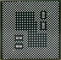
| back image | 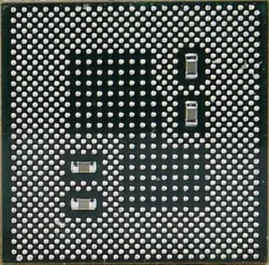 + + |
| base frequency | 1,800 MHz (1.8 GHz, 1,800,000 kHz) +, 2,420 MHz (2.42 GHz, 2,420,000 kHz) + and 2,840 MHz (2.84 GHz, 2,840,000 kHz) + |
| core count | 8 + |
| core name | Kryo 485 Gold + and Kryo 485 Silver + |
| designer | Qualcomm + and ARM Holdings + |
| die area | 73.27 mm² (0.114 in², 0.733 cm², 73,270,000 µm²) + |
| die length | 8.48 mm (0.848 cm, 0.334 in, 8,480 µm) + |
| die width | 8.64 mm (0.864 cm, 0.34 in, 8,640 µm) + |
| dsp | Hexagon 690 DSP + |
| family | Snapdragon 800 + |
| first announced | December 4, 2018 + |
| first launched | January 2019 + |
| full page name | qualcomm/snapdragon 800/855 + |
| has ecc memory support | false + |
| instance of | microprocessor + |
| integrated gpu | Adreno 640 GPU + |
| integrated gpu base frequency | 250 MHz (0.25 GHz, 250,000 KHz) + |
| integrated gpu designer | Qualcomm + |
| integrated gpu max frequency | 585 MHz (0.585 GHz, 585,000 KHz) + |
| isa | ARMv8 + |
| isa family | ARM + |
| l1$ size | 512 KiB (524,288 B, 0.5 MiB) + |
| l1d$ description | 4-way set associative + |
| l1d$ size | 256 KiB (262,144 B, 0.25 MiB) + |
| l1i$ description | 4-way set associative + and 2-way set associative + |
| l1i$ size | 256 KiB (262,144 B, 0.25 MiB) + |
| l2$ description | 8-way set associative + |
| l2$ size | 1 MiB (1,024 KiB, 1,048,576 B, 9.765625e-4 GiB) + and 0.5 MiB (512 KiB, 524,288 B, 4.882812e-4 GiB) + |
| ldate | January 2019 + |
| main image |  + + |
| manufacturer | TSMC + |
| market segment | Mobile + |
| max cpu count | 1 + |
| max memory | 16,384 MiB (16,777,216 KiB, 17,179,869,184 B, 16 GiB, 0.0156 TiB) + |
| max memory bandwidth | 31.79 GiB/s (32,552.96 MiB/s, 34.134 GB/s, 34,134.253 MB/s, 0.031 TiB/s, 0.0341 TB/s) + |
| max memory channels | 8 + |
| microarchitecture | Cortex-A76 + and Cortex-A55 + |
| model number | SDM855 + |
| name | Snapdragon 855 + |
| part number | SM8150 + |
| process | 7 nm (0.007 μm, 7.0e-6 mm) + |
| series | 800 + |
| smp max ways | 1 + |
| supported memory type | LPDDR4X-4266 + |
| technology | CMOS + |
| thread count | 8 + |
| used by | LG G8 ThinQ +, LG V50 ThinQ +, Motorola Moto z3 +, OnePlus 7 Pro +, OPPO Reno +, Samsung Galaxy S10 +, Sony Xperia 1 +, Xiaomi Mi 9 +, Xiaomi Mi MIX 3 + and ZTE Axon 10 Pro + |
| word size | 64 bit (8 octets, 16 nibbles) + |
