| Edit Values | |
| ARM3 µarch | |
| General Info | |
| Arch Type | CPU |
| Designer | Acorn Computers |
| Manufacturer | VLSI Technology, Sanyo |
| Introduction | 1989 |
| Process | 1.5 µm |
| Core Configs | 1 |
| Pipeline | |
| Type | Scalar, Pipelined |
| Stages | 3 |
| Decode | 1-way |
| Instructions | |
| ISA | ARMv2a |
| Cache | |
| L1 Cache | 4 KiB/core 64-way set associative |
| Succession | |
ARM3 is the second-generation commercial ARM implementation designed by Acorn Computers as a successor to the ARM2.
Contents
History
- See also: ARM's History
The ARM3 builds on the success of the ARM2 with higher performance through the introduction of on-die cache but without any major changes to the core itself. The ARM3 was designed by a team of four engineers in nine months and was introduced in 1989. The ARM3 can operate at up to 25 MHz with a peak performance of 25 MIPS and a sustainable performance of 12 MIPS.
Process Technology
- See also: 1.5 µm process
The ARM3 was implemented on a 1.5 µm double-level metal CMOS process.
Architecture
The major goal of the ARM3 was to improve performance. A target of three times the performance of the ARM2 was set. In order to support a faster microprocessor, the system would have to use faster DRAM which would negatively impact the overall cost. Instead, the design team opted to integrating cache.
Key changes from ARM2
- Goal 3x the performance
- Integrated cache
- Integrated clock generator
- Integrated control logic
- Integrated co-processor interface
New instructions
New ARM3 instructions:
Memory:
-
SWP- Swap word memory-register, Atomic (uninterruptible)
Memory Hierarchy
- Cache
- L1 Cache (unified)
- 4 KiB, 64-way set associative
- 16 B line size
- Write-through policy
- Per core
- System DRAM
- Up to 64 MiB
- L1 Cache (unified)
Overview
Control
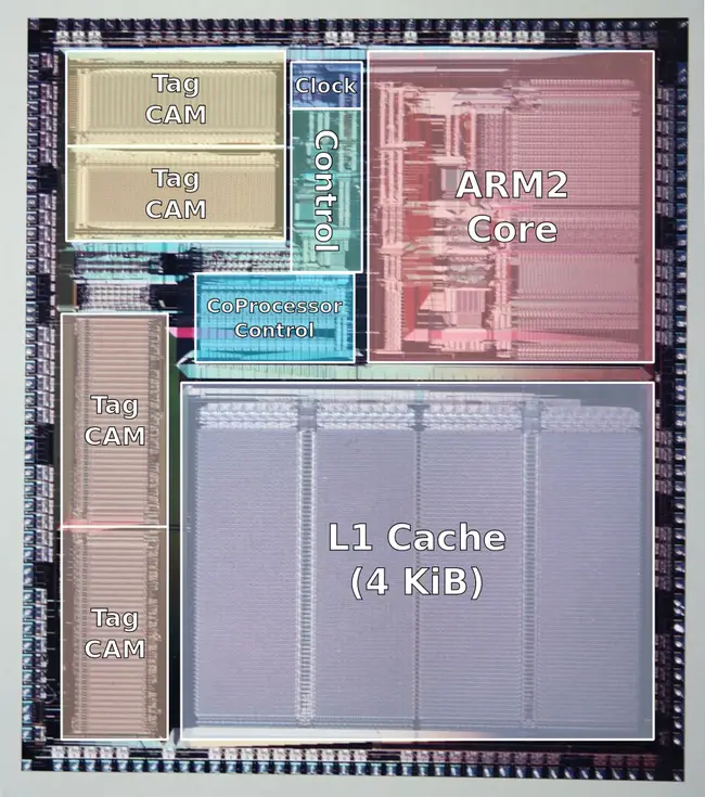
The ARM3's control logic is a state machine implemented as three PLAs. Layout was generated automatically using Psuedo nMOS in order to save on space, albeit at the slight expense of static power dissipation.
Core
Pipeline
- Main article: ARM2 Pipeline
ARM3's pipeline is identical to the ARM2.
Clock Generator
| This section is empty; you can help add the missing info by editing this page. |
Coprocessor Interface
| This section is empty; you can help add the missing info by editing this page. |
Cache
| This section is empty; you can help add the missing info by editing this page. |
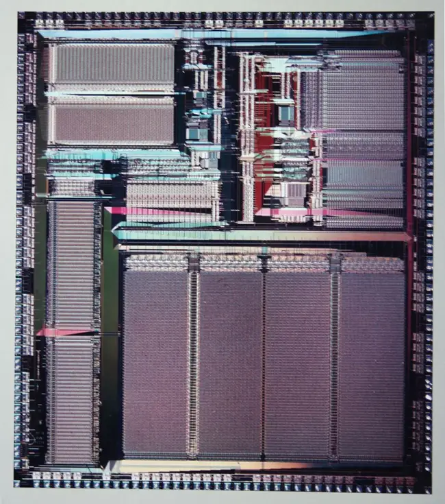
Die
- 12 MHz, 1 W
- 1.5 µm DLM CMOS
- 8.72 mm x 9.95 mm
- 86.764 mm² die size
- 309,656 transistors
- 206,454 SRAM
- 62,973 CAM
- 40,229 logic
- QFP-160
- 119 signal pins
- 41 power/ground pins
All ARM3 Chips
| List of ARM3-based Processors | ||||||||||||
|---|---|---|---|---|---|---|---|---|---|---|---|---|
| Model | Process | Launched | Frequency | Power Dissipation | Max Memory | |||||||
| VL86C020 | ARM3 | 1989 | 20 MHz 0.02 GHz , 25 MHz20,000 kHz 0.025 GHz , 33 MHz25,000 kHz 0.033 GHz , 36 MHz33,000 kHz 0.036 GHz 36,000 kHz | 2 W 2,000 mW 0.00268 hp 0.002 kW | 64 MiB 65,536 KiB 67,108,864 B 0.0625 GiB 6.103516e-5 TiB | |||||||
| Count: 1 | ||||||||||||
References
- Thomas, A. R. P., et al. "A 2nd Generation 32b RISC Processor with 4KByte Cache." Solid-State Circuits Conference, 1989. ESSCIRC'89. Proceedings of the 15th European. IEEE, 1989.
| codename | ARM3 + |
| core count | 1 + |
| designer | Acorn Computers + |
| first launched | 1989 + |
| full page name | acorn/microarchitectures/arm3 + |
| instance of | microarchitecture + |
| instruction set architecture | ARMv2a + |
| manufacturer | VLSI Technology + and Sanyo + |
| microarchitecture type | CPU + |
| name | ARM3 + |
| pipeline stages | 3 + |
| process | 1,500 nm (1.5 μm, 0.0015 mm) + |

