| NNP | |

| |
| Developer | Intel |
| Manufacturer | Intel, TSMC |
| Type | Neural Processors |
| Introduction | May 23, 2018 (announced) 2019 (launch) |
| Process | 28 nm 0.028 μm , 16 nm2.8e-5 mm 0.016 μm , 10 nm1.6e-5 mm 0.01 μm
1.0e-5 mm |
| Technology | CMOS |
| Package | PCIe x16 Gen 3 Card, OCP OAM, M.2 |
| → | |
| Habana HL-Series | |
Neural Network Processors (NNP) is a family of neural processors designed by Intel Nervana for both inference and training.
The NNP family has been discontinued on January 31, 2019, in favor of the Habana HL series.
Contents
Overview
Neural network processors (NNP) is a family of neural processors designed by Intel for the acceleration of artificial intelligence workloads. The name and original architecture originated with the Nervana startup prior to its acquisition by Intel in 2016. Although the first product was announced in 2017, it never made it past customer sampling which eventually served as a learning product. Intel eventually productized those chips starting with their second-generation designs in late 2019.
The NNP family comprises two separate series - NNP-I for inference and NNP-T for training. The two series use entirely different architectures. The training chip is a direct descendent of Nervana's original ASIC design. Those chips use the PCIe and OAM form factors that have high TDPs designed for maximum performance at the data center and for workstations. Unlike the NNP-T, NNP-I inference chips are the product of Intel IDC which, architecturally, are very different from the training chips. They use Intel's low-power client SoC has the base SoC and build the AI architecture from there. The inference chips use low-power PCIe, M.2, and ruler form factors designed for servers, workstations, and embedded applications.
On January 31, 2020, Intel announced that it has discontinued the Nervana NNP product line in favor of the unified architecture it has acquired from Habana Labs a month earlier.
Codenames
| Introduction | Type | Microarchitecture | Process |
|---|---|---|---|
| 20171 | Training | Lake Crest | 28 nm |
| 2019 | Training | Spring Crest | 16 nm |
| 2019 | Inference | Spring Hill | 10 nm |
| 2020 | Training+CPU | Knights Crest | ? |
1 - Only sampled
Training (NNP-T)
Lake Crest
- Main article: Lake Crest µarch
The first generation of NNPs were based on the Lake Crest microarchitecture. Manufactured on TSMC's 28 nm process, those chips were never productized. Samples were used for customer feedback and the design mostly served as a software development vehicle for their follow-up design.
T-1000 Series (Spring Crest)
- Main article: Spring Crest µarch
Launched in late 2019, second-generation NNP-Ts are branded as the NNP T-1000 series and are the first chips to be productized. Fabricated TSMC's 16 nm process based on the Spring Crest microarchitecture, those chips feature a number of enhancements and refinments over the prior generation including a shift from Flexpoint to Bfloat16 and considerable performance uplift. Intel claims that these chips have about 3-4x the training performance of first generation. All NNP-T 1000 chips come with 32 GiB of four HBM2 stacks in a CoWoS package and come in two form factors: PCIe Gen 3 and an OCP OAM accelerator card.
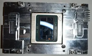
- Proc 16 nm process
- Mem 32 GiB, HBM2-2400
- TDP 300-400 W (150-250 W typical power)
- Perf 108 TOPS (bfloat16)
| List of NNP-T 1000-based Processors | |||||||
|---|---|---|---|---|---|---|---|
| Main processor | Performance | ||||||
| Model | Launched | TDP | EUs | Frequency | HBM2 | Peak Perf (bfloat16) | |
| NNP-T 1300 | 12 November 2019 | 300 W 300,000 mW 0.402 hp 0.3 kW | 22 | 950 MHz 0.95 GHz 950,000 kHz | 32 GiB 32,768 MiB 33,554,432 KiB 34,359,738,368 B 0.0313 TiB | 93.39 TFLOPS 93,390,000,000,000 FLOPS 93,390,000,000 KFLOPS 93,390,000 MFLOPS 93,390 GFLOPS 0.0934 PFLOPS | |
| NNP-T 1400 | 12 November 2019 | 375 W 375,000 mW 0.503 hp 0.375 kW | 24 | 1,100 MHz 1.1 GHz 1,100,000 kHz | 32 GiB 32,768 MiB 33,554,432 KiB 34,359,738,368 B 0.0313 TiB | 108 TFLOPS 108,000,000,000,000 FLOPS 108,000,000,000 KFLOPS 108,000,000 MFLOPS 108,000 GFLOPS 0.108 PFLOPS | |
| Count: 2 | |||||||
POD Reference Design
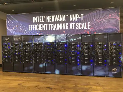
Along with the launch of the NNP-T 1000 series, Intel also introduced the POD reference design. Those systems were intended for large-scale out systems for the processing of very large neural networks. The POD reference design featured 10 racks with 6 nodes per rack. Each of the nodes features eight interconnected OAM cards, producing a system with a total of 480 NNP-Ts.
Inference (NNP-I)
I-1000 Series (Spring Hill)
- Main article: Spring Hill µarch
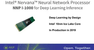
The NNP I-1000 series is Intel's first series of devices designed specifically for the acceleration of inference workloads. Fabricated on Intel's 10 nm process, these chips are based on Spring Hill and incorporate a Sunny Cove core along with twelve specialized inference acceleration engines. The overall SoC design borrows considerable amount of IP from Ice Lake. Those devices come in M.2 and PCIe form factors.
- Proc 10 nm process
- Mem 4x32b LPDDR4x-4200
- TDP 10-50 W
- Eff 2.0-4.8 TOPs/W
- Perf 48-92 TOPS (Int8)
| List of NNP-I-1000-based Processors | |||||
|---|---|---|---|---|---|
| Main processor | Performance | ||||
| Model | Launched | TDP | EUs | Peak Perf (Int8) | |
| NNP-I 1100 | 12 November 2019 | 12 W 12,000 mW 0.0161 hp 0.012 kW | 12 | 50 TOPS 50,000,000,000,000 OPS 50,000,000,000 KOPS 50,000,000 MOPS 50,000 GOPS 0.05 POPS | |
| NNP-I 1300 | 12 November 2019 | 75 W 75,000 mW 0.101 hp 0.075 kW | 24 | 170 TOPS 170,000,000,000,000 OPS 170,000,000,000 KOPS 170,000,000 MOPS 170,000 GOPS 0.17 POPS | |
| Count: 2 | |||||
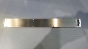
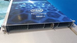
Intel also announced NNP-I in an EDSFF (ruler) form factor which was designed to provide the highest compute density possible for inference. Intel hasn't announced specific models. The rulers were planned t come with a 10-35W TDP range. 32 NNP-Is in a ruler form factor can be packed in a single 1U rack.
See also
| designer | Intel + |
| first announced | May 23, 2018 + |
| first launched | 2019 + |
| full page name | nervana/nnp + |
| instance of | integrated circuit family + |
| main designer | Intel + |
| manufacturer | Intel + and TSMC + |
| name | NNP + |
| package | PCIe x16 Gen 3 Card +, OCP OAM + and M.2 + |
| process | 28 nm (0.028 μm, 2.8e-5 mm) +, 16 nm (0.016 μm, 1.6e-5 mm) + and 10 nm (0.01 μm, 1.0e-5 mm) + |
| technology | CMOS + |
