| Edit Values | |
| Spring Crest µarch | |
| General Info | |
| Arch Type | NPU |
| Designer | Nervana |
| Manufacturer | Intel |
| Introduction | 2019 |
| Process | 16 nm |
| PE Configs | 24 |
| Succession | |
Spring Crest (SCR) is the successor to Lake Crest, a planned neural processor microarchitecture designed by Intel Nervana.
Products based on Spring Crest are branded as the NNP L-1000 series.
Contents
Process Technology
Spring Crest is fabricated on TSMC's 16 nm process.
Architecture
Spring Crest introduces significant improvements over the prior generation.
Key changes from Lake Crest
- 16 nm process (from 28 nm)
- 3x-4x+ performance
- 2x TPCs (24 TPCs, up from 12)
- 33% more InterChip Links (16 ICLs, up from 12)
This list is incomplete; you can help by expanding it.
Block Diagram
Chip
TPC
Overview
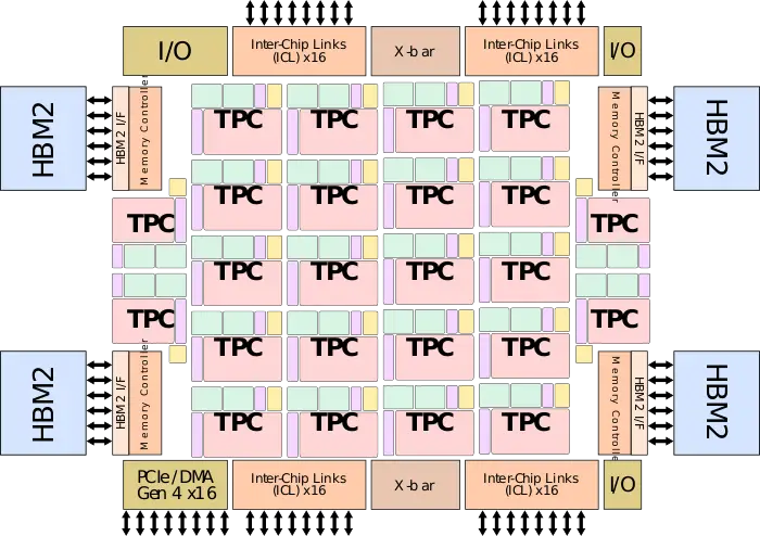
Spring Crest is the successor to Lake Crest, Intel Nervana's first commercial neural processor that made it to mass production. The chip itself is designed for training at the data center. To that end, it's designed as a PCIe Gen 4 x16 accelerator card as well as an OCP Accelerator Module (OAM), targetting air-cooled infrastructure in the 150-250W typical workload power range. Spring Crest is a data center training accelerator, optimized for the fastest time-to-train and highest power efficiency. Emphasis was placed on the reuse of on-die data and batched workloads.
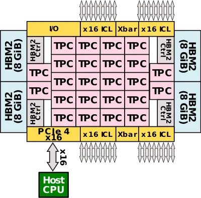
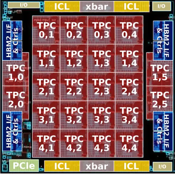
The chip features 24 high-performance tensor processor clusters (TPCs), each incorporating two MAC processing units (MPU) along with a large pool of high-banked high-bandwidth memory. Each of the MPU pairs integrates a 32x32 array for a total of 98,304 FLOPs each cycle for a total of up to 119 TOPS of compute. The MPUs are fed by 60 MiB of distributed SRAM. Spring Crest uses bfloat16 with a 32-bit (SP FP) accumulate. Bandwidth is favored over latency everywhere with the entire chip being linked using a 2D mesh NoC.
Spring Crest is fabricated on TSMC 16-nanometer process and utilizes its CoWoS 2.5D packaging technology to integrate four stack of HBM2 (8Hi) on an interposer for a total capacity of 32 GiB operating at 2400 MT/s.
The chip also exposes four InterChip Links (ICL) ports comprising x16 (4×4) SerDes for a total of 64 SerDes. The ICL ports operate at 112 Gbps for a total bidirectional bandwidth of 3.58 Tbps. Scaling the system with multiple nodes is largely glueless due to the OAM standard. A full system and incorporate up to 1024 Spring Crest processors and behave like one single chip with a consistent programming model designed for both data and model parallelism.
Tensor Processing Cluster (TPC)
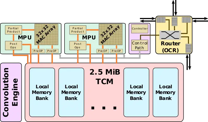
The workhorse component of Spring Crest is the Tensor Processing Cluster (TPC). There are 24 identical instances of the TPC on the die. The TPC comprises four major subsystems: on-chip router (OCR), the control, the MAC processing unit (MPU), and the memory subsystem.
The on-chip router facilitates the data communication between the TPCs as well as shared peripherals such as the PCIe and ICL interfaces.
Control
The control path is responsible for the instruction decode, scheduling of operations, and retiring instructions. Control also coordinates the compute blocks within the TPC. The Spring Crest ISA is a limited instruction set, tensor-based ISA. In other words, all operands are treated as tensors. The ISA comes with many native tensor operations (including more specialized operations such as transpose and tensor slicing). Control includes a microcontroller that allows extending the ISA with custom microcontroller instructions.
MAC Processing Unit (MPU)
There are two compute blocks within each TPC. The processing unit comprises a large matrix multiply array as well as vector operations and specialized deep learning functions. The matrix multiply core is a 32x32 array that uses bfloat16 for the multiply and FP32 for the accumulate. Partial product buffer within the array accumulates partial product in order to reduce memory access and power. Intel selected 32x32 due to the good data reuse that can be achieved with it while keeping it small enough to not lose a lot of performance due to quantization effects.
Outside of the matrix core is the compound vector pipeline that can perform multiple operations on a set of inputs and intermediate values which reduces memory bandwidth and power. Both FP32 and BF16 are supported throughout the entire compound vector pipeline. This also allows for the optimization of non-GEMM operations based on network accuracy requirements. Additionally, the vector pipeline includes specialized optimizations for things such as activation functions, random number generation, reductions, and accumulations. There is also support for programmable FP32 lookup tables.
Memory Subsystem
The memory subsystem is in charge of sourcing and sinking the data with the compute blocks as well as the routing mesh. Each TPC contains 2.5 MiB of local scratchpad memory. With a total of 24 TPCs, there is 60 MiB of scratchpad memory in total on-die. The memory is highly-banked, designed for simultaneous read and write accesses. As part of the memory ports, there is native tensor transpose support. In other words, tensor transpose can be done directly by simply reading and writing into memory without any additional overhead. There is a total of 1.4 Tbps of bandwidth between the compute blocks and the scratchpad memory banks.
Memory is explicitly managed by the software to optimize data locality and data residency - this applies to both the on-die memory and the off-die HBM memory. Hardware management of memory has been kept to a minimum in order to not interfere with software optimizations. Message passing, memory allocation, and memory management are all under software control. The software can also directly transfer memory between TPC as well as HBM and memory banks.
Beyond the on-chip memory, Spring Crest includes four stacks of 8-hi HBM2 memory. The memory operates at 2.4 GT/s for a total bandwidth of 1.23 TB/s and 32 GiB of capacity.
Convolution Engine
As part of the memory subsystem, there is the data transformation convolution engine. The engine is used to reformat the data for convolutions as well as perform some other more general operations such as tensor reshape.
Network-on-Chip (NoC)
Spring Crest integrates a 2-dimensional mesh architecture. The chip has four pods, one at each of the quadrant. Each pod includes six TPCs and is directly linked to the nearest HBM. There are a total of three full-speed bidirectional meshes - for the HBM, external InterChip interconnects, and neighboring pods. The different busses are designed to reduce interference between the different types of traffic. There is a total of 1.3 TB/s of bandwidth in each direction for a total of 2.6 TB/s of cross-sectional bandwidth on the network.
Pod
Within each pod are six TPCs. Each pod is connected to its own HBM, to the external InterChip interconnects (ICLs), and to neighboring pods. Each TPC incorporates a crossbar router going in all three compass directions (North, South, East, and West). The three buses extend from each TPC router in all four directions. There are multiple connections between the meshes and the HBM interface as well as multiple connections to the InterChip Links. In order to exploit parallelism, those buses operate simultaneously and at full speed in order to facilitate many tasks at the same time. For example, some pods may be transferring data to other pods, while some TPCs may be operating on the previous results of another TPC, while another TPC is writing the data back to memory, and another TPC reading memory back on-chip. Software scheduling plays a big role in optimizing network traffic for higher utilization.
Scalability
| This section is empty; you can help add the missing info by editing this page. |
InterChip Link (ICL)
SerDes lanes on Spring Crest are grouped into quads. Each quad operates at 28 GT/s for a total bandwidth of 28 GB/s. Spring Crest features four InterChip Link (ICL) ports. Each ICL comprises four quads for a peak bandwidth of 112 GB/s. In total, with all four ICL ports, Spring Crest has a peak aggregated bandwidth of 448 GB/s (3.584 Tb/s).
Package
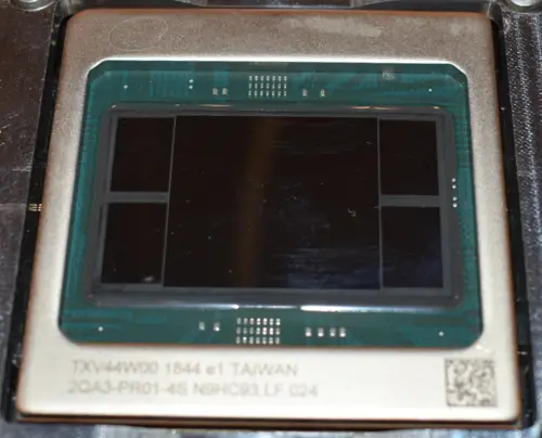
- 60 mm x 60 mm package
- 6-2-6 layer stackup
- BGA with 3,325 pins
- 1 die, 4 HBM 8 GiB stacks
- 1200 mm² CoWoS
PCIe
OAM
Die
- 16 nm process
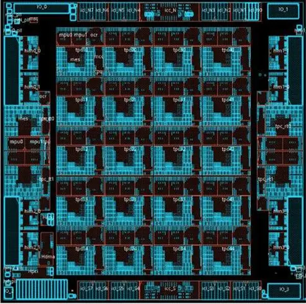
- 680 mm² die size
- 27,000,000,000 transistors
floorplan shown
| codename | Spring Crest + |
| designer | Nervana + and Intel + |
| first launched | 2019 + |
| full page name | nervana/microarchitectures/spring crest + |
| instance of | microarchitecture + |
| manufacturer | Intel + |
| name | Spring Crest + |
| process | 16 nm (0.016 μm, 1.6e-5 mm) + |
| processing element count | 24 + |
