| Edit Values | |
| Spring Crest µarch | |
| General Info | |
| Arch Type | NPU |
| Designer | Nervana |
| Manufacturer | Intel |
| Introduction | 2019 |
| Process | 16 nm |
| PE Configs | 24 |
| Succession | |
Spring Crest (SCR) is the successor to Lake Crest, a planned neural processor microarchitecture designed by Intel Nervana.
Produces based on Spring Crest are branded as the NNP L-1000 series.
Contents
Process Technology
Spring Crest is fabricated on TSMC's 16 nm process.
Architecture
Spring Crest largely builds on the prior generation but introduces more enhancements and compute.
Key changes from Lake Crest
- 16 nm process (from 28 nm)
- 2x computer clusters (24 CCs, up from 12)
- 33% more InterChip Links (16 ICLs, up from 12)
This list is incomplete; you can help by expanding it.
Block Diagram
Chip
TCP
Overview
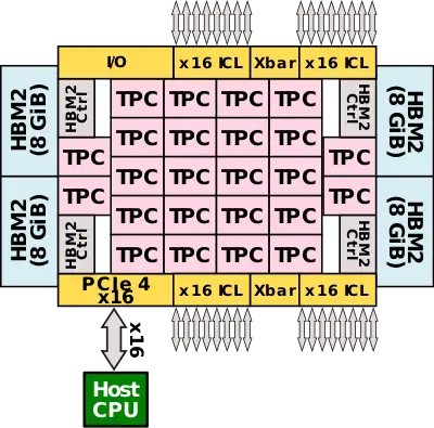
Spring Crest is the successor to Lake Crest, Intel Nervana's first commercial neural processor that made it to mass production. The chip itself is designed for training at the data center. To that end, it's designed as a PCIe Gen 4 x16 accelerator card as well as an OCP Accelerator Module (OAM). Spring Crest is a data center training accelerator, optimized for the fastest time-to-train and highest power efficiency.
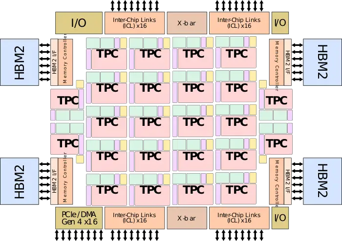
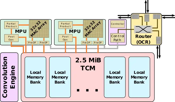
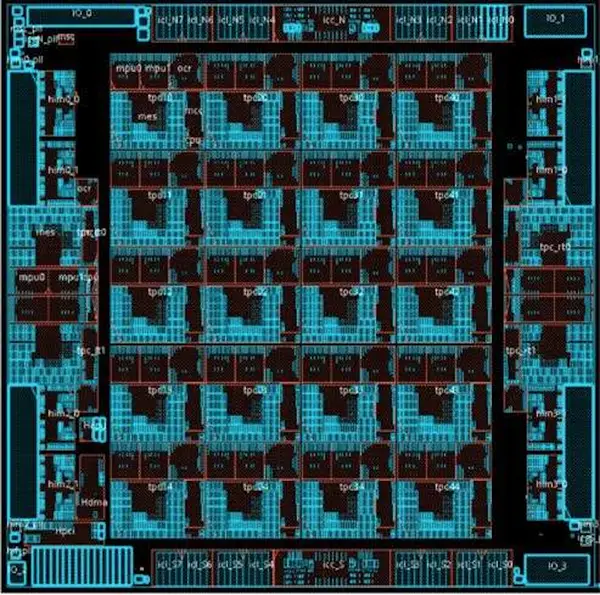
The chip features 24 high-performance tensor processor clusters (TPCs), each incorporating two MAC processing units (MPU) along with a large pool of high-banked high-bandwidth memory. Each of the MPU pairs integrates a 32x32 array for a total of 98,304 FLOPs each cycle. Spring Crest uses bfloat16 with a 32-bit (SP FP) accumulate. Bandwidth is favored over latency everywhere. The entire chip is linked using a 2D mesh NoC.
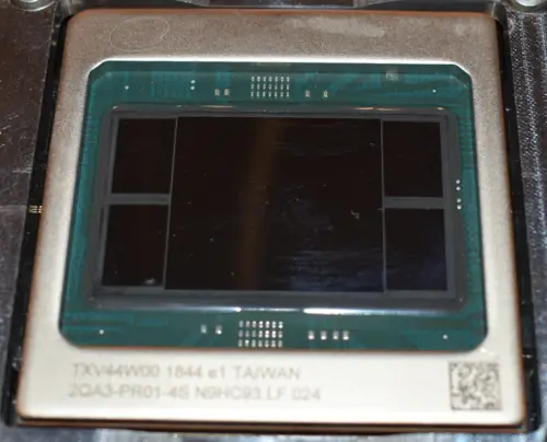
Spring Crest is fabricated on TSMC 16-nanometer process and utilizes its CoWoS packaging technology to integrate four stack of HBM2 (8Hi) on an interposer for a total capacity of 32 GiB operating at 2400 MT/s.
The chip also exposes four InterChip Links (ICL) ports comprising x16 (4×4) SerDes for a total of 64 SerDes. The ICL ports operate at 112 Gbps for a total bidirectional bandwidth of 3.58 Tbps. A full system and incorporate up to 1024 Spring Crest processors and behave like one single chip with a consistent programming model.
Tensor Processing Cluster (TPC)
| This section is empty; you can help add the missing info by editing this page. |
MAC Processing Unit (MPU)
| This section is empty; you can help add the missing info by editing this page. |
Memory Subsystem
| This section is empty; you can help add the missing info by editing this page. |
Network-on-Chip (NoC)
| This section is empty; you can help add the missing info by editing this page. |
Scalability
| This section is empty; you can help add the missing info by editing this page. |
Package
- 60 mm x 60 mm package
- 6-2-6 layer stackup (BGA)
- 3,325 pins
- 1 die, 4 HBM 8 GiB stacks
Die
- 16 nm process
- 680 mm²
- 27,000,000,000 transistors
- 1200 mm² CoWoS
| codename | Spring Crest + |
| designer | Nervana + |
| first launched | 2019 + |
| full page name | nervana/microarchitectures/spring crest + |
| instance of | microarchitecture + |
| manufacturer | Intel + |
| name | Spring Crest + |
| process | 16 nm (0.016 μm, 1.6e-5 mm) + |
| processing element count | 24 + |
