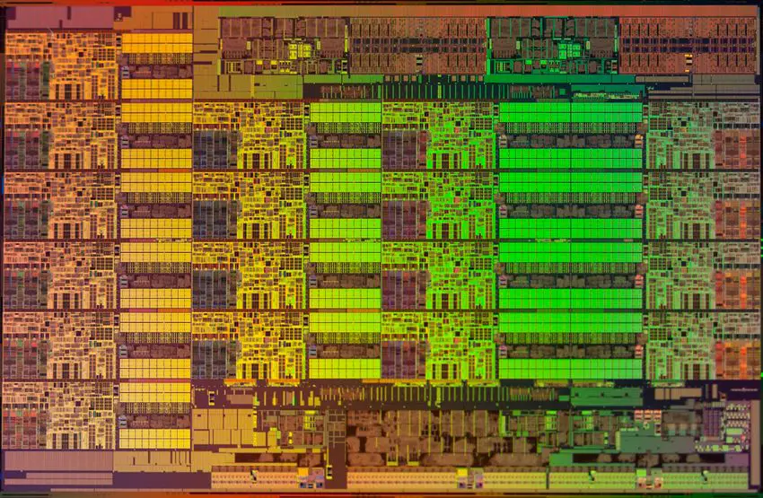
| Edit Values | |
| Haswell µarch | |
| General Info | |
| Arch Type | CPU |
| Designer | Intel |
| Manufacturer | Intel |
| Introduction | June 4, 2013 |
| Phase-out | 2015 |
| Process | 22 nm |
| Core Configs | 2, 4, 6, 8, 16 |
| Pipeline | |
| Type | Superscalar |
| Speculative | Yes |
| Reg Renaming | Yes |
| Stages | 14-19 |
| Instructions | |
| ISA | x86-64 |
| Extensions | MOVBE, MMX, SSE, SSE2, SSE3, SSSE3, SSE4.1, SSE4.2, POPCNT, AVX, AVX2, AES, PCLMUL, FSGSBASE, RDRND, FMA3, BMI, BMI2, F16C, VT-x, VT-d, TXT, TSX |
| Cache | |
| L1I Cache | 32 KB/core 8-way set associative |
| L1D Cache | 32 KB/core 8-way set associative |
| L2 Cache | 256 KB/core 8-way set associative |
| L3 Cache | 1.5 MB/core |
| L4 Cache | 128 MB/package on Iris Pro GPUs only |
| Cores | |
| Core Names | Haswell H, Haswell E, Haswell EP, Haswell EX, Haswell DT, Haswell MB, Haswell ULT, Haswell ULX |
| Succession | |
Haswell (HSW) is Intel's microarchitecture based on the 22 nm process for mobile, desktops, and servers. Haswell, which was introduced in 2013, became the successor to Ivy Bridge. Haswell is named after Haswell, Colorado (Originally Molalla after Molalla, Oregon, it was later renamed due to the difficult pronunciation). In 2014 Intel introduced Haswell's successor, Broadwell.
For desktop and mobile, Haswell is branded as 4th Generation Intel Core processors. For server class processors, Intel branded it as Xeon E3 v3, Xeon E5 v3, and Xeon E7 v3.
Contents
Codenames
| Core | Abbrev | Target |
|---|---|---|
| Haswell DT | HSW-DT | Desktops |
| Haswell MB | HSW-MB | Mobile/Laptops |
| Haswell H | HSW-H | All-in-ones |
| Haswell ULT | HSW-ULT | UltraBooks (MCPs) |
| Haswell ULX | HSW-ULX | Tablets/UltraBooks (SoCs) |
| Haswell EP | HSW-EP | Xeon chips |
| Haswell EX | HSW-EX | Xeon chips, QP |
| Haswell E | HSW-E | High-End Desktops (HEDT) |
Process Technology
- Main article: Ivy Bridge § Process Technology
Haswell-based chips are manufactured on Intel's 22 nm process.
Architecture
While sharing a lot of similarities with its predecessor Ivy Bridge, Haswell introduces many new enhancements and features. Haswell is the first desktop-line of x86s by Intel tailored for a system on chip architecture. This is a significant move that will continue to be developed over the next couple of microarchitectures. Overall Haswell shares the same basic flow as Sandy Bridge and Ivy but expends on them considerably in the execution engine with wider execution units and additional scheduler ports.
Key changes from Ivy Bridge
- 3.5x performance/watt over Nehalem
- Platform Controller Hub (PCH)
- Support for DDR4 (server/enthusiast segments)
- Full Integrated voltage regulator (FIVR)
- New C6 & C7 sleep states
- Cache
- L1D$ has double the bandwidth
- Load: 64B/cycle (up from 32B/cycle)
- Store: 32B/cycle (up from 16B/cycle)
- L2$ bandwidth to L1 is doubled
- 64B/cycle (up from 32B/cycle)
- STLB been made to support 2MB pages
- Table has been doubled to 1,024 entries 8-Way (up from 512, 4-way)
- L1D$ has double the bandwidth
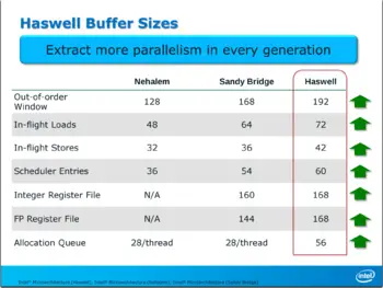
- Reorder Buffer (ROB) was increased to 192 entries (up from 168)
- Scheduler has been widened, (see #Front-end)
- Increased to 60 entries (up from 54)
- Integer register file up 8 entries to 168
- FP register file up 24 entries to 168
- 2 additional execution ports (see #Execution_Units)
- New memory model for Transactional Synchronization Extensions
CPU changes
Haswell can execute more classes of instructions with 4 ops/cycle throughput. SandyBridge/Ivybridge could do so only for NOPs, CLC, some vector MOVs and some zeroing instructions (SUB, XOR and vector analogs).
- MOVSX and MOVZX have 4 op/cycle throughput for 8->32, 8->64 and 16->64 bit forms.
- Some ALU operations have 4 op/cycle throughput for 32-bit registers: XOR, OR, NEG, NOT, although not all (ADD, SUB, CMP and AND don't).
- Variable shifts and rotates (SHL r32, CL etc) latency increased from 1 cycle to 2 cycles, variable SHLD/SHRD from 2 cycles to 4 cycles.
- REP MOVS copy is twice as fast: now ~52 bytes/cycle.
- REP STOS fill is twice as fast: now ~30 bytes/cycle.
GPU changes
- Direct3D 11.1
- OpenGL 4.3
- OpenCL 1.2
- Four versions of GPU options codenamed GT1, GT2, GT3 and GT3 (with GT3e having a dedicated eDRAM L4$)
New instructions
Haswell introduced a number of new instructions:
-
AVX2- Advanced Vector Extensions 2; an extension that extends most integer instructions to 256 bits vectors. -
BMI1- Bit Manipulation Instructions Sets 1 -
BMI2- Bit Manipulation Instructions Sets 2 -
MOVBE- Move Big-Endian instruction -
FMA3- Floating Point Multiply Accumulate, 3 operands -
TSX- Transactional Synchronization Extensions -
INVPCID- Invalidate Process-Context Identifier -
LZCNT- Leading zero count
Block Diagram
Individual Core
Memory Hierarchy
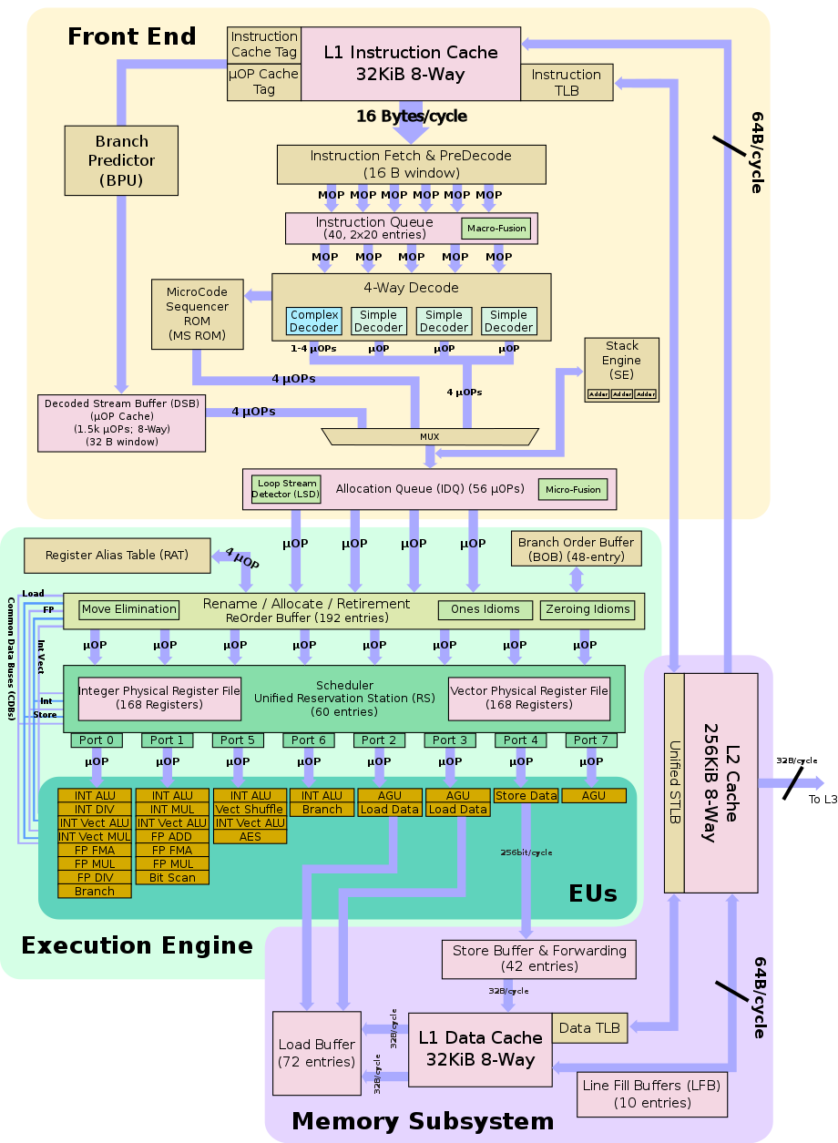
The memory hierarchy in Haswell had a number of changes from its predecessor. The cache bandwidth for both load and store have been doubled (64B/cycle for load and 32B/cycle for store; up from 32/16 respectively). Significant enhancements have been done to support the new gather instructions and transactional memory. With Haswell new port 7 which adds an address generation for stores, up to two loads and one store are possible each cycle.
- Cache
- L1I Cache:
- 32 KB 8-way set associative
- 64 B line size
- Write-back policy
- shared by the two threads, per core
- 32 KB 8-way set associative
- L1D Cache:
- 32 KB 8-way set associative
- 64 B line size
- shared by the two threads, per core
- 4 cycles for fastest load-to-use
- 64 Bytes/cycle load bandwidth
- 32 Bytes/cycle store bandwidth
- Write-back policy
- 32 KB 8-way set associative
- L2 Cache:
- unified, 256 KB 8-way set associative
- 11 cycles for fastest load-to-use
- 64B/cycle bandwidth to L1$
- Write-back policy
- L3 Cache:
- 1.5 - 3 MB
- Write-back policy
- Per core
- L4 Cache:
- 128 MB
- Per package
- Only on the Iris Pro GPUs
- L1I Cache:
Haswell TLB consists of dedicated level one TLB for instruction cache and another one for data cache. Additionally there is a unified second level TLB.
- TLBs:
- ITLB
- 4KB page translations:
- 128 entries; 4-way set associative
- dynamic partition; divided between the two threads
- 2MB/4MB page translations:
- 8 entries; fully associative
- Duplicated for each thread
- 4KB page translations:
- DTLB
- 4KB page translations:
- 64 entries; 4-way set associative
- fixed partition; divided between the two threads
- 2MB/4MB page translations:
- 32 entries; 4-way set associative
- 1G page translations:
- 4 entries; 4-way set associative
- 4KB page translations:
- STLB
- 4KB+2M page translations:
- 1024 entries; 8-way set associative
- shared
- 4KB+2M page translations:
- ITLB
Core
Pipeline
Haswell, like its predecessor Ivy Bridge, also has a dual-threaded and out-of-order pipeline.
Front-end
The front-end is the complicated part of the microarchitecture as it deals with variable length x86 instructions ranging from 1 to 15 bytes. The main goal here is to fetch and decode correctly the next set of instructions. The caches have not changed in Haswell from Ivy Bridge, with the L1i$ still 32KB , 8-way set associative shared dynamically by the two threads. Instruction cache instruction fetching remains 16B/cycle. TLB is also still 128-entries, 4-way for 4KB pages and 8-entries, fully associative for 2MB page mode. The fetched instructions are then moved on to an instruction queue which has 40 entries, 20 for each thread. Haswell continued to improve the branch misses although the exact details have not been made public.
Haswell has the same µOps cache as Ivy Bridge - 1,536 entries organized in 32 sets of 8 cache lines with 6 µOps each. Hits can yield up to 4-µOps/cycle. The cache supports microcoded instructions (being pointers to ROM entries). Cache is shared by the two threads.
Following the instruction queue, instructions are coded via the complex 4-way decoder. The decoder has 3 simple decoders and 1 complex decoder. In total, they are capable of emitting 3 single fused µOps and an additional 1-4 fused µOps. The unit handles both micro and macro fusions. Macro-fusion as a result of compatible adjacent µOps may be merged into a single µOp. Push and pops as well as call and return are also handled at this stage. 4 instructions, but with the aid of the macro-fusion, up to 5 instructions can be decoded each cycle.
Execution engine
Continuing with the decoder is the register renaming stage. This is crucial for out-of-order execution. In this stage the architectural x86 registers get mapped into one of the many physical registers. The integer physical register file (PRF) has been enlarged by 8 addition registers for a total 168. Likewise the FP PRF was extended by 24 registers bringing it too to 168 registers. The larger increase in the FP PRF is likely to accommodate the new AVX2 extension. The ROB in Haswell has been increased to 192 entries (from 168 in Ivy) where each entry corresponds to a single µOp. The ROB is fixed split between the two threads. Additional scheduler resources get allocated as well - this includes stores, loads, and branch buffer entries. Note that due to how dependencies are handled, there may be more or less µOps than what was fed in. For the most part, the renamer is unified and deals with both integers and vectors. Resources, however, are partitioned between the two threads. Finally, as a last step, the µOps are matched with a port depending on their intended execution purpose. Up to 4 fused µOps may be renamed and handled per thread per cycle. Both the load and store in-flight units were increased to 72 and 42 entries respectively.
Haswell continues to use a unified scheduler for all µOps which holds 60 entries. µOps at this stage sit idle until they are cleared to be executed via their assigned dispatch port. µOps may be held due to resource unavailability.
Following a successful execution, µOps retire at a rate of up to 4 fused µOps/cycle. Retirement is once again in-order and frees up any reserved resource (ROB entries, PRFs entries, and various other buffers).
Execution Units
Some of the biggest architectural changes were done in the area of the execution units. Haswell widened the scheduler by two ports - one new integer dispatch port and a new memory port bringing the total to 8 µOps/cycle. The various ports have also been rebalanced. The new port 6 adds another Integer ALU designs to improve integer workloads freeing up Port 0 and 1 for vector works. It also adds a second branch unit to low the congestion Port 0. The second port that was added, Port 7 adds a new AGU. This is largely due to the improvements for AVX2 that roughly doubled its throughput. Port 0 had its ALU/Mul/shifter extended to 256-bits; same is true for the vector ALU on port 1 and the ALU/shuffle on port 5. Additionally a 256-bit FMA unit were added to both port 0 and port 1. The change makes it possible for FMAs and FMULs to issue on both ports. In theory, Haswell can peak at over double the performance of Sandy Bridge, with 16 double / 32 single precision FLOP/cycle + Integer ALU option + Vector operation.
The scheduler dispatches up to 8 ready µOps/cycle in FIFO order through the dispatch ports. µOps involving computational operations are sent to ports 0, 1, 5, and 6 to the appropriate unit. Likewise ports 2, 3, 4 and 7 are used for load/store and address calculations.
Clock domains
| This section is empty; you can help add the missing info by editing this page. |
Overclocking
- See also: Intel's XMP
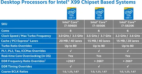
Overclocking needs to be done on an unlocked part such as the Core i7-5820K, Core i7-5930K, or Core i7-5960X Extreme Edition. Additionally those chips need to be paired with the Intel X99 Chipset.
The 5930K and the 5820K are hexa-core parts whereas the 5960X is an octa-core part. Between 28 and 40 PCIe lanes are possible with a core ratio of up to x80 the BCLK.
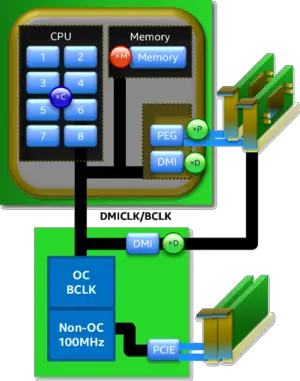
Haswell provides a Coarsed BCLK ratios of either 100 MHz, 125 MHz, or 167 MHz (this was consequently changed in Skylake). The clock is generated internally by the chipset, but motherboard ODMs could generate it independently. A single BCLK from the PCH is fed in < 1 MHz steps, however in practice the input is very much limited by PCI Express and DMI PLL interface. This works out to 100 MHz ± 5-7% PEG/DMI @ 5:5, 125 MHz ±5-7% PEG/DMI @ 5:4, and 166.66 MHz ±5-7% @ 5:3.
- fCORE = BCLK × [Core Ratio]
- fRING = BCLK × [Ring Ratio]
- FDDR = BCLK × [1.33/1.00] × [DDR Ratio]
All the clock domains in Haswell are derived from the BCLK (also called DMICLK). In the diagram on the right (xC) refers to the Core Frequency and is represented as a multiple of BCLK (Core Frequency = BCLK × Core Freq Multiplier up to x80). Likewise (xM) refers to the memory ratio (up to 2667 MT/s in granularity operations of 200 and 266 MHz) and Two additional multipliers to adjust the PEG(PCIe & Graphics)/DMI links which should remain at a nominal frequency of 100 MHz.
Voltage control is done by Haswell's new FIVER (Full Integrated Voltage Regulator) based architecture. This means that voltage arrives via the VCCin input from the motherboard into the processor and onto the voltage regulator (VCCin = SVID 1.8 V Nom up to 2.3 V+). Internally, the various voltage planes are all derived from there. This includes the VCORE, VRING, and VSA. With the memory voltage (VDDQ = 1.2 V Nom) provided from the motherboard with to its own rail.
Die
Client Die
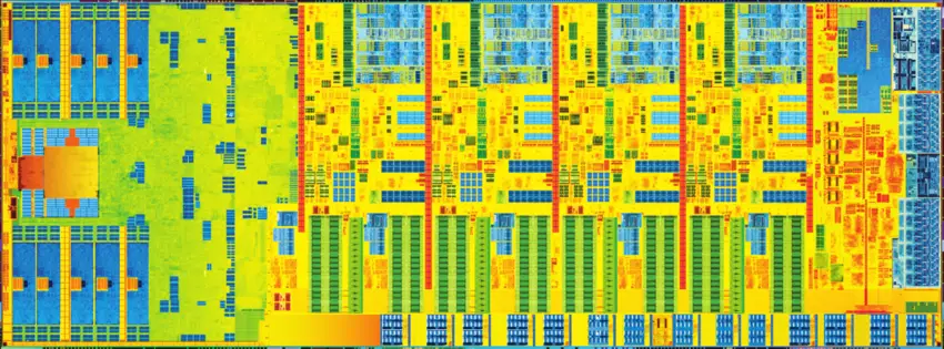
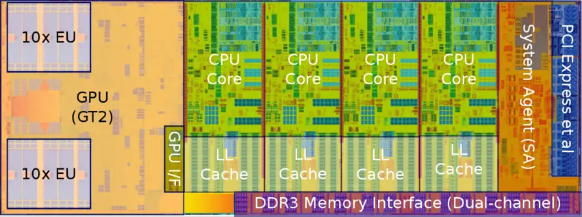
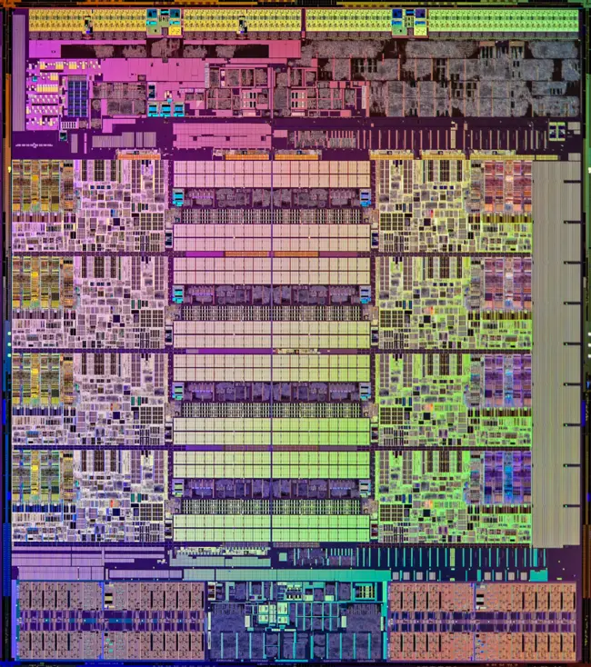
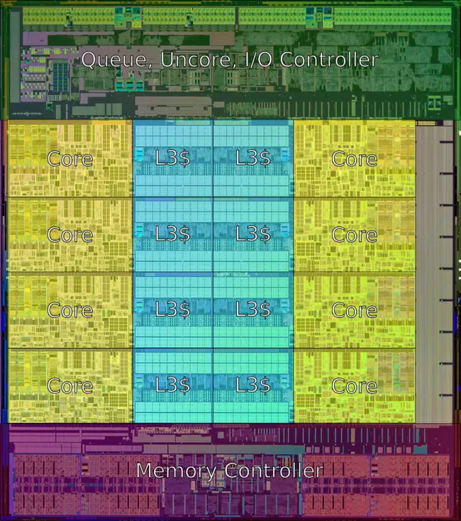
Client die come in 2, 4, or 8 cores setup with dual/quad being mainstream models and the octa-core being the high-end desktop.
Dual-core
- 22 nm process
- 960,000,000 transistors
- 131 mm² die size, (I believe this is actually 181mm2, note the large graphics unit compared to quad-core)
- 2 CPU cores
Quad-core
- 22 nm process
- 1,400,000,000 transistors
- 177 mm² die size
- 4 CPU cores
- 1 GPU core
- 2x10xEU (80 ALUs)
Octa-core
- Core i7-5960X
- Octa-core processor
- 22 nm process
- 2,600,000,000 transistors
- 355.52 mm² die size
- 17.6 mm x 20.2 mm
Server Die
Octadeca-core
- 18 cores processor
- 22 nm process
- 5,690,000,000 transistors
- 622 mm² die size
Added instructions
AVX2 - Integer data types were extended to 256-bit SIMD.
- VBROADCASTI128
- VBROADCASTSD
- VBROADCASTSS
- VEXTRACTI128
- VGATHERDPD
- VGATHERDPS
- VGATHERQPD
- VGATHERQPS
- VINSERTI128
- VMOVNTDQA
- VMPSADBW
- VPABSB
- VPABSD
- VPABSW
- VPACKSSDW
- VPACKSSWB
- VPACKUSDW
- VPACKUSWB
- VPADDB
- VPADDD
- VPADDQ
- VPADDSB
- VPADDSW
- VPADDUSB
- VPADDUSW
- VPADDW
- VPALIGNR
- VPAND
- VPANDN
- VPAVGB
- VPAVGW
- VPBLENDD
- VPBLENDVB
- VPBLENDW
- VPBROADCASTB
- VPBROADCASTD
- VPBROADCASTQ
- VPBROADCASTW
- VPCMPEQB
- VPCMPEQD
- VPCMPEQQ
- VPCMPEQW
- VPCMPGTB
- VPCMPGTD
- VPCMPGTQ
- VPCMPGTW
- VPERM2I128
- VPERMD
- VPERMPD
- VPERMPS
- VPERMQ
- VPGATHERDD
- VPGATHERDQ
- VPGATHERQD
- VPGATHERQQ
- VPHADDD
- VPHADDSW
- VPHADDW
- VPHSUBD
- VPHSUBSW
- VPHSUBW
- VPMADDUBSW
- VPMADDWD
- VPMASKMOVD
- VPMASKMOVQ
- VPMAXSB
- VPMAXSD
- VPMAXSW
- VPMAXUB
- VPMAXUD
- VPMAXUW
- VPMINSB
- VPMINSD
- VPMINSW
- VPMINUB
- VPMINUD
- VPMINUW
- VPMOVMSKB
- VPMOVSXBD
- VPMOVSXBQ
- VPMOVSXBW
- VPMOVSXDQ
- VPMOVSXWD
- VPMOVSXWQ
- VPMOVZXBD
- VPMOVZXBQ
- VPMOVZXBW
- VPMOVZXDQ
- VPMOVZXWD
- VPMOVZXWQ
- VPMULDQ
- VPMULHRSW
- VPMULHUW
- VPMULHW
- VPMULLD
- VPMULLW
- VPMULUDQ
- VPOR
- VPSADBW
- VPSHUFB
- VPSHUFD
- VPSHUFHW
- VPSHUFLW
- VPSIGNB
- VPSIGND
- VPSIGNW
- VPSLLD
- VPSLLDQ
- VPSLLQ
- VPSLLVD
- VPSLLVQ
- VPSLLW
- VPSRAD
- VPSRAVD
- VPSRAW
- VPSRLD
- VPSRLDQ
- VPSRLQ
- VPSRLVD
- VPSRLVQ
- VPSRLW
- VPSUBB
- VPSUBD
- VPSUBQ
- VPSUBSB
- VPSUBSW
- VPSUBUSB
- VPSUBUSW
- VPSUBW
- VPUNPCKHBW
- VPUNPCKHDQ
- VPUNPCKHQDQ
- VPUNPCKHWD
- VPUNPCKLBW
- VPUNPCKLDQ
- VPUNPCKLQDQ
- VPUNPCKLWD
- VPXOR
BMI1 / BMI2 - Bit Manipulation Instructions Sets
FMA3 - Fused Multiply-Add instructions, 3 operands
- VFMADD123PD
- VFMADD123PS
- VFMADD123SD
- VFMADD123SS
- VFMADD132PD
- VFMADD132PS
- VFMADD132SD
- VFMADD132SS
- VFMADD213PD
- VFMADD213PS
- VFMADD213SD
- VFMADD213SS
- VFMADD231PD
- VFMADD231PS
- VFMADD231SD
- VFMADD231SS
- VFMADD312PD
- VFMADD312PS
- VFMADD312SD
- VFMADD312SS
- VFMADD321PD
- VFMADD321PS
- VFMADD321SD
- VFMADD321SS
- VFMADDSUB123PD
- VFMADDSUB123PS
- VFMADDSUB132PD
- VFMADDSUB132PS
- VFMADDSUB213PD
- VFMADDSUB213PS
- VFMADDSUB231PD
- VFMADDSUB231PS
- VFMADDSUB312PD
- VFMADDSUB312PS
- VFMADDSUB321PD
- VFMADDSUB321PS
- VFMSUB123PD
- VFMSUB123PS
- VFMSUB123SD
- VFMSUB123SS
- VFMSUB132PD
- VFMSUB132PS
- VFMSUB132SD
- VFMSUB132SS
- VFMSUB213PD
- VFMSUB213PS
- VFMSUB213SD
- VFMSUB213SS
- VFMSUB231PD
- VFMSUB231PS
- VFMSUB231SD
- VFMSUB231SS
- VFMSUB312PD
- VFMSUB312PS
- VFMSUB312SD
- VFMSUB312SS
- VFMSUB321PD
- VFMSUB321PS
- VFMSUB321SD
- VFMSUB321SS
- VFMSUBADD123PD
- VFMSUBADD123PS
- VFMSUBADD132PD
- VFMSUBADD132PS
- VFMSUBADD213PD
- VFMSUBADD213PS
- VFMSUBADD231PD
- VFMSUBADD231PS
- VFMSUBADD312PD
- VFMSUBADD312PS
- VFMSUBADD321PD
- VFMSUBADD321PS
- VFNMADD123PD
- VFNMADD123PS
- VFNMADD123SD
- VFNMADD123SS
- VFNMADD132PD
- VFNMADD132PS
- VFNMADD132SD
- VFNMADD132SS
- VFNMADD213PD
- VFNMADD213PS
- VFNMADD213SD
- VFNMADD213SS
- VFNMADD231PD
- VFNMADD231PS
- VFNMADD231SD
- VFNMADD231SS
- VFNMADD312PD
- VFNMADD312PS
- VFNMADD312SD
- VFNMADD312SS
- VFNMADD321PD
- VFNMADD321PS
- VFNMADD321SD
- VFNMADD321SS
- VFNMSUB123PD
- VFNMSUB123PS
- VFNMSUB123SD
- VFNMSUB123SS
- VFNMSUB132PD
- VFNMSUB132PS
- VFNMSUB132SD
- VFNMSUB132SS
- VFNMSUB213PD
- VFNMSUB213PS
- VFNMSUB213SD
- VFNMSUB213SS
- VFNMSUB231PD
- VFNMSUB231PS
- VFNMSUB231SD
- VFNMSUB231SS
- VFNMSUB312PD
- VFNMSUB312PS
- VFNMSUB312SD
- VFNMSUB312SS
- VFNMSUB321PD
- VFNMSUB321PS
- VFNMSUB321SD
- VFNMSUB321SS
MOVBE - Move Big-Endian instruction
TSX - Transactional Synchronization Extensions
Cores
| This section is empty; you can help add the missing info by editing this page. |
All Haswell Chips
| List of Haswell Processors | |||||||||||||||||||
|---|---|---|---|---|---|---|---|---|---|---|---|---|---|---|---|---|---|---|---|
| Main processor | Turbo Boost | Mem | IGP | ||||||||||||||||
| Model | Launched | Price | Family | Core Name | Cores | Threads | L2$ | L3$ | TDP | Frequency | 1 Core | 2 Cores | 3 Cores | 4 Cores | Max Mem | GPU | Frequency | Turbo | |
| i5-4570R | 4 June 2013 | Core i5 | 4 | 4 | 1 MiB 1,024 KiB 1,048,576 B 9.765625e-4 GiB | 4 MiB 4,096 KiB 4,194,304 B 0.00391 GiB | 65 W 65,000 mW 0.0872 hp 0.065 kW | 2.7 GHz 2,700 MHz 2,700,000 kHz | 3.2 GHz 3,200 MHz 3,200,000 kHz | 3.1 GHz 3,100 MHz 3,100,000 kHz | 3 GHz 3,000 MHz 3,000,000 kHz | 3 GHz 3,000 MHz 3,000,000 kHz | 32 GiB 32,768 MiB 33,554,432 KiB 34,359,738,368 B 0.0313 TiB | Intel Iris Pro Graphics 5200 | 200 MHz 0.2 GHz 200,000 KHz | 1,150 MHz 1.15 GHz 1,150,000 KHz | |||
| i5-4670R | 4 June 2013 | Core i5 | 4 | 4 | 1 MiB 1,024 KiB 1,048,576 B 9.765625e-4 GiB | 4 MiB 4,096 KiB 4,194,304 B 0.00391 GiB | 65 W 65,000 mW 0.0872 hp 0.065 kW | 3 GHz 3,000 MHz 3,000,000 kHz | 3.7 GHz 3,700 MHz 3,700,000 kHz | 3.6 GHz 3,600 MHz 3,600,000 kHz | 3.5 GHz 3,500 MHz 3,500,000 kHz | 3.5 GHz 3,500 MHz 3,500,000 kHz | 32 GiB 32,768 MiB 33,554,432 KiB 34,359,738,368 B 0.0313 TiB | Intel Iris Pro Graphics 5200 | 200 MHz 0.2 GHz 200,000 KHz | 1,300 MHz 1.3 GHz 1,300,000 KHz | |||
| i7-4750HQ | 2 June 2013 | Core i7 | 4 | 8 | 1 MiB 1,024 KiB 1,048,576 B 9.765625e-4 GiB | 6 MiB 6,144 KiB 6,291,456 B 0.00586 GiB | 47 W 47,000 mW 0.063 hp 0.047 kW | 2 GHz 2,000 MHz 2,000,000 kHz | 3.2 GHz 3,200 MHz 3,200,000 kHz | 3.1 GHz 3,100 MHz 3,100,000 kHz | 3 GHz 3,000 MHz 3,000,000 kHz | 3 GHz 3,000 MHz 3,000,000 kHz | 32 GiB 32,768 MiB 33,554,432 KiB 34,359,738,368 B 0.0313 TiB | Intel Iris Pro Graphics 5200 | 200 MHz 0.2 GHz 200,000 KHz | 1,200 MHz 1.2 GHz 1,200,000 KHz | |||
| i7-4760HQ | 14 April 2014 | Core i7 | 4 | 8 | 1 MiB 1,024 KiB 1,048,576 B 9.765625e-4 GiB | 6 MiB 6,144 KiB 6,291,456 B 0.00586 GiB | 47 W 47,000 mW 0.063 hp 0.047 kW | 2.1 GHz 2,100 MHz 2,100,000 kHz | 3.3 GHz 3,300 MHz 3,300,000 kHz | 3.2 GHz 3,200 MHz 3,200,000 kHz | 3.1 GHz 3,100 MHz 3,100,000 kHz | 3.1 GHz 3,100 MHz 3,100,000 kHz | 32 GiB 32,768 MiB 33,554,432 KiB 34,359,738,368 B 0.0313 TiB | Intel Iris Pro Graphics 5200 | 200 MHz 0.2 GHz 200,000 KHz | 1,200 MHz 1.2 GHz 1,200,000 KHz | |||
| i7-4770HQ | 20 July 2014 | Core i7 | 4 | 8 | 1 MiB 1,024 KiB 1,048,576 B 9.765625e-4 GiB | 6 MiB 6,144 KiB 6,291,456 B 0.00586 GiB | 47 W 47,000 mW 0.063 hp 0.047 kW | 2.2 GHz 2,200 MHz 2,200,000 kHz | 3.4 GHz 3,400 MHz 3,400,000 kHz | 3.3 GHz 3,300 MHz 3,300,000 kHz | 3.2 GHz 3,200 MHz 3,200,000 kHz | 3.2 GHz 3,200 MHz 3,200,000 kHz | 32 GiB 32,768 MiB 33,554,432 KiB 34,359,738,368 B 0.0313 TiB | Intel Iris Pro Graphics 5200 | 200 MHz 0.2 GHz 200,000 KHz | 1,200 MHz 1.2 GHz 1,200,000 KHz | |||
| i7-4770R | 4 June 2013 | Core i7 | 4 | 8 | 1 MiB 1,024 KiB 1,048,576 B 9.765625e-4 GiB | 6 MiB 6,144 KiB 6,291,456 B 0.00586 GiB | 47 W 47,000 mW 0.063 hp 0.047 kW | 3.2 GHz 3,200 MHz 3,200,000 kHz | 3.9 GHz 3,900 MHz 3,900,000 kHz | 3.8 GHz 3,800 MHz 3,800,000 kHz | 3.7 GHz 3,700 MHz 3,700,000 kHz | 3.7 GHz 3,700 MHz 3,700,000 kHz | 32 GiB 32,768 MiB 33,554,432 KiB 34,359,738,368 B 0.0313 TiB | Intel Iris Pro Graphics 5200 | 200 MHz 0.2 GHz 200,000 KHz | 1,300 MHz 1.3 GHz 1,300,000 KHz | |||
| i7-4850EQ | 20 February 2014 | Core i7 | 4 | 8 | 1 MiB 1,024 KiB 1,048,576 B 9.765625e-4 GiB | 6 MiB 6,144 KiB 6,291,456 B 0.00586 GiB | 47 W 47,000 mW 0.063 hp 0.047 kW | 1.6 GHz 1,600 MHz 1,600,000 kHz | 3.2 GHz 3,200 MHz 3,200,000 kHz | 3.1 GHz 3,100 MHz 3,100,000 kHz | 3 GHz 3,000 MHz 3,000,000 kHz | 3 GHz 3,000 MHz 3,000,000 kHz | 32 GiB 32,768 MiB 33,554,432 KiB 34,359,738,368 B 0.0313 TiB | Intel Iris Pro Graphics 5200 | 200 MHz 0.2 GHz 200,000 KHz | 650 MHz 0.65 GHz 650,000 KHz | |||
| i7-4850HQ | 4 June 2013 | Core i7 | 4 | 8 | 1 MiB 1,024 KiB 1,048,576 B 9.765625e-4 GiB | 6 MiB 6,144 KiB 6,291,456 B 0.00586 GiB | 47 W 47,000 mW 0.063 hp 0.047 kW | 2.3 GHz 2,300 MHz 2,300,000 kHz | 3.5 GHz 3,500 MHz 3,500,000 kHz | 3.4 GHz 3,400 MHz 3,400,000 kHz | 3.3 GHz 3,300 MHz 3,300,000 kHz | 3.3 GHz 3,300 MHz 3,300,000 kHz | 32 GiB 32,768 MiB 33,554,432 KiB 34,359,738,368 B 0.0313 TiB | Intel Iris Pro Graphics 5200 | 200 MHz 0.2 GHz 200,000 KHz | 1,200 MHz 1.2 GHz 1,200,000 KHz | |||
| i7-4860EQ | 20 February 2014 | Core i7 | 4 | 8 | 1 MiB 1,024 KiB 1,048,576 B 9.765625e-4 GiB | 6 MiB 6,144 KiB 6,291,456 B 0.00586 GiB | 47 W 47,000 mW 0.063 hp 0.047 kW | 1.8 GHz 1,800 MHz 1,800,000 kHz | 3.2 GHz 3,200 MHz 3,200,000 kHz | 3.1 GHz 3,100 MHz 3,100,000 kHz | 3 GHz 3,000 MHz 3,000,000 kHz | 3 GHz 3,000 MHz 3,000,000 kHz | 32 GiB 32,768 MiB 33,554,432 KiB 34,359,738,368 B 0.0313 TiB | Intel Iris Pro Graphics 5200 | 200 MHz 0.2 GHz 200,000 KHz | 750 MHz 0.75 GHz 750,000 KHz | |||
| i7-4860HQ | 19 January 2014 | Core i7 | 4 | 8 | 1 MiB 1,024 KiB 1,048,576 B 9.765625e-4 GiB | 6 MiB 6,144 KiB 6,291,456 B 0.00586 GiB | 47 W 47,000 mW 0.063 hp 0.047 kW | 2.3 GHz 2,300 MHz 2,300,000 kHz | 2.4 GHz 2,400 MHz 2,400,000 kHz | 3.6 GHz 3,600 MHz 3,600,000 kHz | 3.5 GHz 3,500 MHz 3,500,000 kHz | 3.4 GHz 3,400 MHz 3,400,000 kHz | 32 GiB 32,768 MiB 33,554,432 KiB 34,359,738,368 B 0.0313 TiB | Intel Iris Pro Graphics 5200 | 200 MHz 0.2 GHz 200,000 KHz | 1,200 MHz 1.2 GHz 1,200,000 KHz | |||
| i7-4870HQ | 20 July 2014 | Core i7 | 4 | 8 | 1 MiB 1,024 KiB 1,048,576 B 9.765625e-4 GiB | 6 MiB 6,144 KiB 6,291,456 B 0.00586 GiB | 47 W 47,000 mW 0.063 hp 0.047 kW | 2.5 GHz 2,500 MHz 2,500,000 kHz | 3.7 GHz 3,700 MHz 3,700,000 kHz | 3.6 GHz 3,600 MHz 3,600,000 kHz | 3.5 GHz 3,500 MHz 3,500,000 kHz | 3.5 GHz 3,500 MHz 3,500,000 kHz | 32 GiB 32,768 MiB 33,554,432 KiB 34,359,738,368 B 0.0313 TiB | Intel Iris Pro Graphics 5200 | 200 MHz 0.2 GHz 200,000 KHz | 1,200 MHz 1.2 GHz 1,200,000 KHz | |||
| i7-4950HQ | 4 June 2013 | Core i7 | 4 | 8 | 1 MiB 1,024 KiB 1,048,576 B 9.765625e-4 GiB | 6 MiB 6,144 KiB 6,291,456 B 0.00586 GiB | 47 W 47,000 mW 0.063 hp 0.047 kW | 2.4 GHz 2,400 MHz 2,400,000 kHz | 3.6 GHz 3,600 MHz 3,600,000 kHz | 3.5 GHz 3,500 MHz 3,500,000 kHz | 3.4 GHz 3,400 MHz 3,400,000 kHz | 3.4 GHz 3,400 MHz 3,400,000 kHz | 32 GiB 32,768 MiB 33,554,432 KiB 34,359,738,368 B 0.0313 TiB | Intel Iris Pro Graphics 5200 | 200 MHz 0.2 GHz 200,000 KHz | 1,300 MHz 1.3 GHz 1,300,000 KHz | |||
| i7-4960HQ | 1 September 2013 | Core i7 | 4 | 8 | 1 MiB 1,024 KiB 1,048,576 B 9.765625e-4 GiB | 6 MiB 6,144 KiB 6,291,456 B 0.00586 GiB | 47 W 47,000 mW 0.063 hp 0.047 kW | 2.6 GHz 2,600 MHz 2,600,000 kHz | 3.8 GHz 3,800 MHz 3,800,000 kHz | 3.7 GHz 3,700 MHz 3,700,000 kHz | 3.6 GHz 3,600 MHz 3,600,000 kHz | 3.4 GHz 3,400 MHz 3,400,000 kHz | 32 GiB 32,768 MiB 33,554,432 KiB 34,359,738,368 B 0.0313 TiB | Intel Iris Pro Graphics 5200 | 200 MHz 0.2 GHz 200,000 KHz | 1,300 MHz 1.3 GHz 1,300,000 KHz | |||
| i7-4980HQ | 1 September 2014 | Core i7 | 4 | 8 | 1 MiB 1,024 KiB 1,048,576 B 9.765625e-4 GiB | 6 MiB 6,144 KiB 6,291,456 B 0.00586 GiB | 47 W 47,000 mW 0.063 hp 0.047 kW | 2.8 GHz 2,800 MHz 2,800,000 kHz | 4 GHz 4,000 MHz 4,000,000 kHz | 3.9 GHz 3,900 MHz 3,900,000 kHz | 3.6 GHz 3,600 MHz 3,600,000 kHz | 3.6 GHz 3,600 MHz 3,600,000 kHz | 32 GiB 32,768 MiB 33,554,432 KiB 34,359,738,368 B 0.0313 TiB | Intel Iris Pro Graphics 5200 | 200 MHz 0.2 GHz 200,000 KHz | 1,300 MHz 1.3 GHz 1,300,000 KHz | |||
| i7-4930MX | 2 June 2013 | Core i7EE | Haswell | 4 | 8 | 1 MiB 1,024 KiB 1,048,576 B 9.765625e-4 GiB | 8 MiB 8,192 KiB 8,388,608 B 0.00781 GiB | 57 W 57,000 mW 0.0764 hp 0.057 kW | 3 GHz 3,000 MHz 3,000,000 kHz | 3.9 GHz 3,900 MHz 3,900,000 kHz | 3.8 GHz 3,800 MHz 3,800,000 kHz | 3.7 GHz 3,700 MHz 3,700,000 kHz | 3.7 GHz 3,700 MHz 3,700,000 kHz | 32 GiB 32,768 MiB 33,554,432 KiB 34,359,738,368 B 0.0313 TiB | Intel HD Graphics 4600 | 400 MHz 0.4 GHz 400,000 KHz | 1,350 MHz 1.35 GHz 1,350,000 KHz | ||
| i7-4940MX | 19 January 2014 | Core i7EE | Haswell | 4 | 8 | 1 MiB 1,024 KiB 1,048,576 B 9.765625e-4 GiB | 8 MiB 8,192 KiB 8,388,608 B 0.00781 GiB | 57 W 57,000 mW 0.0764 hp 0.057 kW | 3.1 GHz 3,100 MHz 3,100,000 kHz | 4 GHz 4,000 MHz 4,000,000 kHz | 3.9 GHz 3,900 MHz 3,900,000 kHz | 3.8 GHz 3,800 MHz 3,800,000 kHz | 3.8 GHz 3,800 MHz 3,800,000 kHz | 32 GiB 32,768 MiB 33,554,432 KiB 34,359,738,368 B 0.0313 TiB | Intel HD Graphics 4600 | 400 MHz 0.4 GHz 400,000 KHz | 1,350 MHz 1.35 GHz 1,350,000 KHz | ||
| i7-5960X | 29 August 2014 | Core i7EE | Haswell E | 8 | 16 | 2 MiB 2,048 KiB 2,097,152 B 0.00195 GiB | 20 MiB 20,480 KiB 20,971,520 B 0.0195 GiB | 140 W 140,000 mW 0.188 hp 0.14 kW | 3 GHz 3,000 MHz 3,000,000 kHz | 3.5 GHz 3,500 MHz 3,500,000 kHz | 3.5 GHz 3,500 MHz 3,500,000 kHz | 3.3 GHz 3,300 MHz 3,300,000 kHz | 3.3 GHz 3,300 MHz 3,300,000 kHz | 64 GiB 65,536 MiB 67,108,864 KiB 68,719,476,736 B 0.0625 TiB | |||||
| E3-1284L v3 | 1 October 2014 | Xeon E3 | 4 | 8 | 1 MiB 1,024 KiB 1,048,576 B 9.765625e-4 GiB | 6 MiB 6,144 KiB 6,291,456 B 0.00586 GiB | 47 W 47,000 mW 0.063 hp 0.047 kW | 1.8 GHz 1,800 MHz 1,800,000 kHz | 3.2 GHz 3,200 MHz 3,200,000 kHz | 3.1 GHz 3,100 MHz 3,100,000 kHz | 3 GHz 3,000 MHz 3,000,000 kHz | 3 GHz 3,000 MHz 3,000,000 kHz | 32 GiB 32,768 MiB 33,554,432 KiB 34,359,738,368 B 0.0313 TiB | Intel Iris Pro Graphics 5200 | 200 MHz 0.2 GHz 200,000 KHz | 750 MHz 0.75 GHz 750,000 KHz | |||
| Count: 19 | |||||||||||||||||||
References
- Hammarlund, Per, et al. "Haswell: The fourth-generation intel core processor." IEEE Micro 34.2 (2014): 6-20.
- Dan Ragland, Overclocking System Architect, 2015 IDF, in San Francisco, Session RPCS001 ("Overclocking 6th Generation Intel® Core™ Processors!"), August 18, 2015
Documents
| codename | Haswell + |
| core count | 2 +, 4 +, 6 +, 8 +, 10 +, 12 +, 14 +, 16 + and 18 + |
| designer | Intel + |
| first launched | June 4, 2013 + |
| full page name | intel/microarchitectures/haswell (client) + |
| instance of | microarchitecture + |
| instruction set architecture | x86-64 + |
| manufacturer | Intel + |
| microarchitecture type | CPU + |
| name | Haswell + |
| phase-out | 2015 + |
| pipeline stages (max) | 19 + |
| pipeline stages (min) | 14 + |
| process | 22 nm (0.022 μm, 2.2e-5 mm) + |
