From WikiChip
Exynos 8895 - Samsung
| Edit Values | |
| Exynos 8895 | |
| General Info | |
| Designer | Samsung, ARM Holdings |
| Manufacturer | Samsung |
| Model Number | 8895 |
| Market | Mobile |
| Introduction | February 23, 2017 (announced) March 29, 2017 (launched) |
| General Specs | |
| Family | Exynos |
| Series | Exynos 9 |
| Locked | No |
| Frequency | 2314 MHz, 1690 MHz |
| Microarchitecture | |
| ISA | ARMv8 (ARM) |
| Microarchitecture | M2, Cortex-A53 |
| Core Name | Exynos M2, Cortex-A53 |
| Process | 10 nm |
| Technology | CMOS |
| MCP | Yes |
| Word Size | 64 bit |
| Cores | 8 |
| Threads | 8 |
| Max Memory | 8 GiB |
| Multiprocessing | |
| Max SMP | 1-Way (Uniprocessor) |
| Electrical | |
| Vcore | 0.905 V-1.22 V |
| TDP | 5 W |
| cTDP down | 12 W |
| cTDP down frequency | 2314 MHz |
| cTDP up | 16 W |
| cTDP up frequency | 2810 MHz |
| OP Temperature | -15 °C – 115 °C |
| Tjunction | 115 – 115 |
| Succession | |
| Contemporary | |
| Exynos 9820 | |
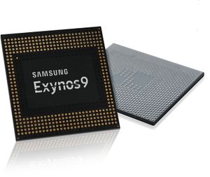
Exynos 8895 is a 64-bit octa-core ARM high performance mobile system on a chip designed by Samsung and introduced in mid-2019. The processor is fabricated on Samsung's 10nm EUV (Extreme Ultra Violet) FinFET process and features 8 cores in a tri-cluster configuration consisting of 4 Mongoose 2 big cores running at 2314 to 2810 MHz, 4 Cortex-A53 little cores at 1690 to 2002 MHz. This chip supports up to 8 GiB of dual-channel 16-bit LPDDR4X-1794 memory and incorporates a Mali-G71 MP20 GPU. The 8895 incorporates an LTE modem supporting cat 16 download and upload.
Cache
- Main articles: Mongoose 2 § Cache and Cortex-A53 § Cache
For the Mongoose 2 core cluster:
|
Cache Organization
Cache is a hardware component containing a relatively small and extremely fast memory designed to speed up the performance of a CPU by preparing ahead of time the data it needs to read from a relatively slower medium such as main memory. The organization and amount of cache can have a large impact on the performance, power consumption, die size, and consequently cost of the IC. Cache is specified by its size, number of sets, associativity, block size, sub-block size, and fetch and write-back policies. Note: All units are in kibibytes and mebibytes. |
|||||||||||||||||||||||||||||||||||||
|
|||||||||||||||||||||||||||||||||||||
For the Cortex-A53 cluster:
|
Cache Organization
Cache is a hardware component containing a relatively small and extremely fast memory designed to speed up the performance of a CPU by preparing ahead of time the data it needs to read from a relatively slower medium such as main memory. The organization and amount of cache can have a large impact on the performance, power consumption, die size, and consequently cost of the IC. Cache is specified by its size, number of sets, associativity, block size, sub-block size, and fetch and write-back policies. Note: All units are in kibibytes and mebibytes. |
|||||||||||||||||||||||||
|
|||||||||||||||||||||||||
Memory controller
|
Integrated Memory Controller
|
||||||||||||||||||
|
||||||||||||||||||
Graphics
|
Integrated Graphics Information
|
||||||||||||||||||||||||||||||||||||
|
||||||||||||||||||||||||||||||||||||
| Codec | Encode | Decode150 |
|---|---|---|
| HEVC (H.265) | ✔ | ✔ |
| MPEG-4 AVC (H.264) | ✔ | ✔ |
| VP9 | ✔ | ✔ |
All at 4K UHD 60fps.
Wireless
| Cellular | |||||||
| 4G |
| ||||||
|---|---|---|---|---|---|---|---|
ISP
- 28MP Rear
- 16MP Front
- 28MP+28MP Dual
Features
[Edit/Modify Supported Features]
|
Supported ARM Extensions & Processor Features
|
||||||||
|
||||||||
Utilizing devices
- Samsung Galaxy Note 8
- Samsung Galaxy S8
- Samsung Galaxy S8+
Facts about "Exynos 8895 - Samsung"
| base frequency | 2,314 MHz (2.314 GHz, 2,314,000 kHz) + and 1,700 MHz (1.7 GHz, 1,700,000 kHz) + |
| core count | 8 + |
| core name | Exynos M2 + and Cortex-A53 + |
| designer | Samsung + and ARM Holdings + |
| die area | 103.64 mm² (0.161 in², 1.036 cm², 103,640,000 µm²) + |
| family | Exynos + |
| first announced | February 23, 2017 + |
| first launched | March 29, 2017 + |
| full page name | samsung/exynos/8895 + |
| instance of | microprocessor + |
| isa | ARMv8 + |
| isa family | ARM + |
| ldate | March 29, 2017 + |
| main image |  + + |
| manufacturer | Samsung + |
| market segment | Mobile + |
| max cpu count | 1 + |
| microarchitecture | Mongoose 2 + and Cortex-A53 + |
| model number | 8895 + |
| name | Exynos 8895 + |
| process | 10 nm (0.01 μm, 1.0e-5 mm) + |
| series | Exynos 9 + |
| smp max ways | 1 + |
| technology | CMOS + |
| thread count | 8 + |
| word size | 64 bit (8 octets, 16 nibbles) + |