| Edit Values |
| Xavier |
|
| Designer | Nvidia |
| Manufacturer | TSMC |
| Market | Artificial Intelligence |
| Introduction | January 8, 2018 (announced) |
|
| Family | Tegra |
|
| ISA | ARMv8 (ARM) |
| Process | 12 nm |
| Transistors | 9,000,000,000 |
| Technology | CMOS |
| Die | 350 mm² |
| Word Size | 64 bit |
| Cores | 8 |
| Threads | 8 |
|
| TDP | 30 W |
| TDP (Typical) | 20 W |
Tegra Xavier is a 64-bit ARM high-performance autonomous machine system on a chip designed by Nvidia and introduced in 2018. Xavier is incorporated into Nvidia's Drive Pegasus, Jetson, and a number of other autonomous computer.
Overview
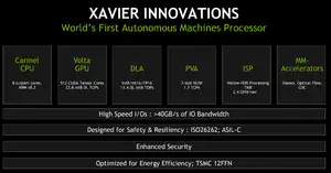
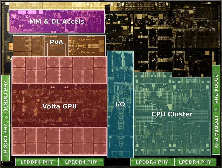
Xavier is an autonomous machine process designed by Nvidia and introduced at CES 2018. Silicon came back in the last week of December 2017 with sampling started in the first quarter of 2018. NVIDIA plans on mass production by the end of the year. NVIDIA reported that the product is a result of $2 billion R&D and 8,000 engineering years. The chip is said to have full redundancy and diversity in its functional blocks. The chip itself comprises an eight-core CPU cluster, GPU, deep learning accelerator, vision accelerator, ISP, and a set of multimedia accelerators.
Architecture
CPU
- Main article: Carmel core
The chip features eight Carmel core, Nvidia's own custom 64-bit ARM cores.
GPU
- Main article: Volta
The chip incorporates a Volta GPU with 512 CUDA Cores capable of operating in 64-bit and 32-bit floating point as well as 8-bit integer. This allows the various deep learning artificial neural networks types to run efficiently in the format most suitable for them. This translates to 1.3 CUDA TOPS (32-bit FP) and another 20 Tensor Core TOPS (16-bit FP).
Accelerators
Xavier incorporates a Programmable Vision Accelerator (PVA) for processing computer vision. It is capable of 1.6 TOPS and the ability to do stereo disparity (e.g., processing parallax between two cameras to obtain useful information such as depth), optical flow (e.g., direction and speed of vectors), and image processing. Additionally, since the chip is expected to be connected to a network of cameras (e.g., side, front, inside), the chip is capable of doing real-time encoding for all camera in high dynamic range.
| Video Processing
|
| Encode |
Decode
|
| 1.2 GPIX/s |
1.8 GPIX/s
|
The chip has an ISP with native full-range HDR support and tile rendering capable of processing at 1.5 GPIX/s.
Deep Learning Accelerator
The chip incorporates a deep learning accelerator (DLA) that implements a number of specific set of deep learning functions common to many applications. This allows them to read the highest possible energy efficiency for those operations. The DLA has a peak performance of 5 TOPS for 16-bit integers or 10 TOPS for 8-bit integer.
Memory controller
[Edit/Modify Memory Info]
 |
Integrated Memory Controller
|
| Max Type | LPDDR4-2133 |
|---|
| Supports ECC | Yes |
|---|
| Channels | 8 |
|---|
| Width | 32 bit |
|---|
| Max Bandwidth | 127.1 GiB/s 130,150.4 MiB/s
136.473 GB/s
136,472.586 MB/s
0.124 TiB/s
0.136 TB/s
|
|---|
|
I/O
- 16 CSI channels
- 1x gE interface
- 1x 10gE interface
Die
SoC
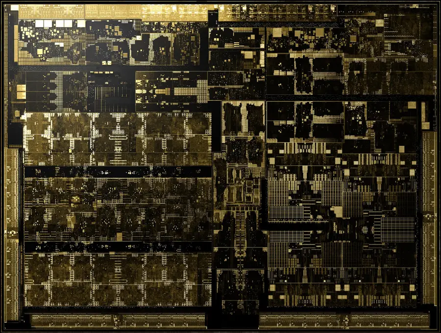
- 9,000,000,000 transistors
- 350 mm² die size
- TSMC's 12FFN


GPU
CPU
PVA
MM Engine / DLA
Southbridge
Documents
