Semiconductor & Computer Engineering
| Edit Values | |
| Xavier | |
 | |
| General Info | |
| Designer | Nvidia |
| Manufacturer | TSMC |
| Model Number | Tegra194 |
| Market | Artificial Intelligence, Embedded |
| Introduction | January 8, 2018 (announced) June, 2018 (launched) |
| General Specs | |
| Family | Tegra |
| Microarchitecture | |
| ISA | ARMv8 (ARM) |
| Microarchitecture | Carmel, Volta |
| Core Name | Carmel |
| Process | 12 nm |
| Transistors | 9,000,000,000 |
| Technology | CMOS |
| Die | 350 mm² |
| Word Size | 64 bit |
| Cores | 8 |
| Threads | 8 |
| Multiprocessing | |
| Max SMP | 4-Way (Multiprocessor) |
| Electrical | |
| TDP | 30 W |
| TDP (Typical) | 20 W |
Tegra Xavier is a 64-bit ARM high-performance system on a chip for autonomous machines designed by Nvidia and introduced in 2018. Xavier is incorporated into a number of Nvidia's computers including the Jetson Xavier, Drive Xavier, and the Drive Pegasus.
Contents
Overview[edit]

Xavier is an autonomous machine processor designed by Nvidia and introduced at CES 2018. Silicon came back in the last week of December 2017 with sampling started in the first quarter of 2018. NVIDIA plans on mass production by the end of the year. NVIDIA reported that the product is a result of $2 billion R&D and 8,000 engineering years. The chip is said to have full redundancy and diversity in its functional blocks.

The design targets and architecture started back in 2014. Fabricated on TSMC 12 nm process, the chip itself comprises an eight-core CPU cluster, GPU with additional inference optimizations, deep learning accelerator, vision accelerator, and a set of multimedia accelerators providing additional support for machine learning (stereo, LDC, optical flow). The ISP has been enhanced to provide native HDR support, higher precision math without offloading work to the GPU. Xavier features a large set of I/O and has been designed for safety and reliability supporting various standards such as Functional safety ISO-26262 and ASIL level C. The CPU cluster is fully cache coherent and the coherency is extended to all the other accelerators on-chip.
At the platform level, one of the bigger changes took place at the I/O subsystem. Xavier features NVLink 1.0 supporting 20 GB/s in each direction for connecting a discrete graphics processor to Xavier in a cache coherent manner. Xavier has PCIe Gen 4.0 support (16 GT/s). It's worth noting that Xavier added support for an end-point mode in addition to the standard root complex support. This support meant they can connect two Xaviers directly one to another (2-way multiprocessing) without going through a PCIe switch or alike.
Architecture[edit]
CPU[edit]

- Main article: Carmel core
The chip features eight control/management Carmel cores, Nvidia's own custom 64-bit ARM cores. Those cores implement ARMv8.2 with RAS support and safety built-in, including dual-execution mode. The cluster consists of 4 duplexes, each sharing 2 MiB of L2 cache. All cores are fully cache coherent which is extended to the GPU and all the other accelerators in the chip. Compared to Parker which was based on Denver 2, Nividia reports around 2x the multithreaded performance.
GPU[edit]

- Main article: Volta
Xavier implements a derivative of their Volta GPU with a set of finer changes to address the machine learning market, particularly improving inference performance over training. It has eight Volta stream multiprocessors along with their standard 128 KiB of L1 cache and a 512 KiB of shared L2. Compared to Parker, Nvidia claims this GPU has 2.1x the graphics performance. Whereas their desktop parts (e.g., GV100) are a very powerful GPU that is used for training, the GPU here is optimized for inference. The most obvious change is that each Volta multiprocessor contains eight tensor cores, each of which can perform 64x FP16 MACs or 128x INT8 MACs per cycle. All of this yields a maximum 22.6 tera-operations (int8) per second.
| Throughput |
|---|
| 22.6 DL TOPS 8-bit |
| 2.8 CUDA TFLOPS FP16 |
| 1.4 CUDA TFLOPS FP32 |
Accelerators[edit]
Xavier incorporates a set of accelerators designed to augment the functionality offered by the GPU and CPU in order to provide added flexibility and perhaps offer a way to implement some of the more common set of algorithms slightly more efficiently.
Programmable Vision Accelerator[edit]

Xavier incorporates a Programmable Vision Accelerator (PVA) for processing computer vision. There are actually two exact instances of the PVA on-chip, each can be used in lock-step or independently and are capable of implementing some of the common filter loop and other detection algorithms (e.g. Harris corner, FFTs). For each of the PVAs, there is a Cortex-R5 core along with two dedicated vector processing units, each with its own memory and DMA. The DMA on the PVA is designed to operate on tiles of memory. To that end, the DMA performs the address calculation and can perform prefetching while the processing pipes operate. This is 7-slot VLIW architecture made of 2 scalar slots, 2 vector slots, and 3 memory operations. The pipe is 256 bit wide (slightly wider because of the guard bits keeping the precision for the operation) and all types can operate at full throughput (32x8b, 16x16b, and 8x32b vector math). The pipe supports additional operations beyond vector such as custom logic for table lookup and hardware looping.
| Throughput |
|---|
| 1.7 CV TOPS |
It's worth noting that since the chip is expected to be connected to a network of cameras (e.g., side, front, inside), the PVA is capable of doing real-time encoding for all camera in high dynamic range.
| Video Processing | |
|---|---|
| Encode | Decode |
| 1.2 GPIX/s | 1.8 GPIX/s |
The chip has an ISP with native full-range HDR support and tile rendering capable of processing at 1.5 GPIX/s.
Deep Learning Accelerator[edit]
The other accelerators on-die is the deep learning accelerator (DLA) which is actually a physical implementation of the open source Nvidia NVDLA architecture. Xavier has two instances of NVDLA which can offer a peak theoretical performance of 5.7 teraFLOPS (half precision FP) or twice the throughput at 11.4 TOPS for int8.
| Throughput |
|---|
| 11.4 TOPS (int8) |
| 5.7 TFLOPS (FP16) |
Stereo & Optical Flow Engine[edit]
Xavier has dedicated engines for stereo and optical flow
| Throughput |
|---|
| 12.4 TOPS 8-bit |
| 6.2 TOPS 16-bit |
Memory controller[edit]
|
Integrated Memory Controller
|
||||||||||
|
||||||||||
I/O[edit]
- NVLINK
- NVLINK 1.0 (20 GB/s)
- PCIE
- Multiple 16GT/s gen4 controllers
- x8, x4, x2, x1 configurations
- Root port + Endpoint
- USB
- 3x USB3.1 (10 GT/s) ports
- 4x USB2.0 ports
- DISPLAY
- 4x DP/HDMI/eDP
- 4K @ 60 Hz
- DP HBR3
- HDMI 2.0
- CAMERA
- 16 CSI lanes
- 40 Gbps in DPHY 1.2 Mode
- 109 Gbps in CPHY 1.1 Mode
- OTHER
- Ethernet
- CAN
- UART
- UFS
- SDMMC
- SPIO
- I2C
- I2S
- GPIO
Die[edit]
SoC[edit]

.png)
GPU[edit]
- ~89.2 mm² silicon area

.png)
CPU[edit]
See Carmel § CPU Complex.
PVA[edit]

.png)
MM Engine / DLA[edit]
- ~21.75 mm² silicon area

Board[edit]
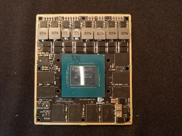
Jetson Xavier, front
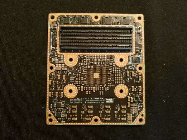
Jetson Xavier, back
.png)
.png)
Documents[edit]
See also[edit]
- Tesla FSD Chip
Bibliography[edit]
- IEEE Hot Chips 30 Symposium (HCS) 2018.
- Schor, David. (September, 2018). "Hot Chips 30: Nvidia Xavier SoC"
| core count | 8 + |
| core name | Carmel + |
| designer | Nvidia + |
| die area | 350 mm² (0.543 in², 3.5 cm², 350,000,000 µm²) + |
| family | Tegra + |
| first announced | January 8, 2018 + |
| first launched | June 2018 + |
| full page name | nvidia/tegra/xavier + |
| has ecc memory support | true + |
| instance of | microprocessor + |
| isa | ARMv8 + |
| isa family | ARM + |
| ldate | June 2018 + |
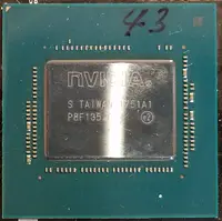
| main image |  + + |
| manufacturer | TSMC + |
| market segment | Artificial Intelligence + and Embedded + |
| max cpu count | 4 + |
| max memory bandwidth | 127.1 GiB/s (130,150.4 MiB/s, 136.473 GB/s, 136,472.586 MB/s, 0.124 TiB/s, 0.136 TB/s) + |
| max memory channels | 8 + |
| microarchitecture | Carmel + and Volta + |
| model number | Tegra194 + |
| name | Xavier + |
| process | 12 nm (0.012 μm, 1.2e-5 mm) + |
| smp max ways | 4 + |
| supported memory type | LPDDR4X-4266 + |
| tdp | 30 W (30,000 mW, 0.0402 hp, 0.03 kW) + |
| tdp (typical) | 20 W (20,000 mW, 0.0268 hp, 0.02 kW) + |
| technology | CMOS + |
| thread count | 8 + |
| transistor count | 9,000,000,000 + |
| word size | 64 bit (8 octets, 16 nibbles) + |