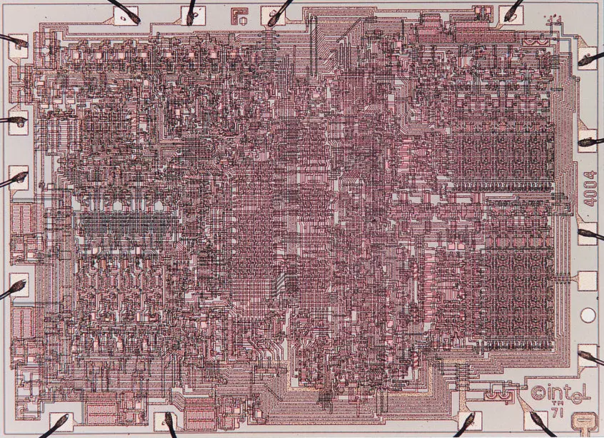
Template:mpu The Intel 4004 was released by Intel Corporation in 1971 and was the first commercially available microprocessor. The 4004 was a 4-bit CPU, designed for use in the Busicom 141-PF printing calculator[1]. The chip, which is clocked at 740 KHz, employs a 10µm[2] process silicon-gate, capable of executing 92,000 instructions per second. The chip was capable of accessing 4KB of program memory and 640 bytes of RAM. The 4004 was part of the Intel MCS-4 system.
The microprocessor had a limited architecture, such as: only a 3-levels deep stack, a complex memory access scheme, and no interrupt support. In 1974 Intel released an enhanced version of the chip called the 4040.
Variations
Three primary source variations were produced by Intel: C4004, D4004 and the P4004. The Intel C4004 was the first chip to be manufactured; it had the gray traces visible on the white ceramic package itself. The C4004 was produced up until mid 1976, when production for the Intel D4004 began. The D4004 had a plastic, black ceramic package. The Intel P4004 is the plastic packaging version.
A couple secondary sources exists, which has been developed by National Semiconductor and Hitachi since mid-1975. National Semiconductor produced two versions: INS4004J and INS4004D. The INS4004J is a 16-pin black, ceramic DIP, while the INS4004D version is a 16-pin side-brazed, ceramic DIP. The other source was the HD35404 made by Hitachi. A third source was Microsystems International which actually manufactured an enhanced version of the chip since mid 1970 (also introduced in 1971).
| Manufacturer | Model | Package |
|---|---|---|
| Intel | C4004 | 16-pin Ceramic DIP |
| Intel | D4004 | 16-pin Ceramic DIP |
| Intel | P4004 | 16-pin Plastic DIP |
| National Semiconductor | INS4004D | 16-pin Ceramic DIP |
| National Semiconductor | INS4004J | 16-pin side-brazed Ceramic DIP |
| Hitachi | HD35404 | 16-pin DIP |
| Microsystems International | MF7114 | ? |
Pinout
The 4004 has 16 pins that are used for i/o, memory controller, clock phases, power and reset.
| Pin # | Pin Name | Purpose | Explanation |
|---|---|---|---|
| 1 | D0 | Bidirectional data bus pins | Address and data communication to the ROM and RAM occurs on D0-D3. |
| 2 | D1 | ||
| 3 | D2 | ||
| 4 | D3 | ||
| 5 | Vss | Main Supply | |
| 6 | Clock Phase 1 | Clock inputs | |
| 7 | Clock Phase 2 | ||
| 8 | Sync | ROM & RAM Sync | Synchronizes the ROM and RAM by signaling the clock is on the raising edge. |
| 9 | Reset | Reset flag | A logic 1 clears all processor status registers and forces the program counter to jump to address 0x0. The RESET signal must be on for at least 64 clock cycles in order to take effect. |
| 10 | Test | Test logic state | Signal can be tested via the JCN instruction.
|
| 11 | CM-ROM | CM-ROM output | ROM selection signal used to retrieve data from memory. |
| 12 | VDD | VSS -15±5% | |
| 13 | CM-RAM3 | CM-ROM outputs | Bank selection signal for the 4002 RAM chips in the system. |
| 14 | CM-RAM2 | ||
| 15 | CM-RAM1 | ||
| 16 | CM-RAM0 |
Designers
Lead designers for the 4004 are:
- Ted Hoff
- Federico Faggin
- Stan Mazor
- Masatoshi Shim
Die Shot
- 10 µm process
- pMOS transistors
- 2,250 transistors
- 12 mm² die


