| Line 7: | Line 7: | ||
|introduction=February 20, 2019 | |introduction=February 20, 2019 | ||
|process=7 nm | |process=7 nm | ||
| + | |cores=4 | ||
| + | |cores 2=8 | ||
| + | |cores 3=16 | ||
| + | |cores 4=32 | ||
| + | |cores 5=64 | ||
| + | |cores 6=96 | ||
| + | |cores 7=128 | ||
| + | |type=Superscalar | ||
| + | |type 2=Superpipeline | ||
|oooe=Yes | |oooe=Yes | ||
|speculative=Yes | |speculative=Yes | ||
|renaming=Yes | |renaming=Yes | ||
| + | |stages=11 | ||
| + | |decode=4-way | ||
| + | |isa=ARMv8.2 | ||
| + | |l1i=64 KiB | ||
| + | |l1i per=core | ||
| + | |l1i desc=4-way set associative | ||
| + | |l1d=64 KiB | ||
| + | |l1d per=core | ||
| + | |l1d desc=4-way set associative | ||
| + | |l2=512-1 MiB | ||
| + | |l2 per=core | ||
| + | |l2 desc=8-way set associative | ||
| + | |l3=2-4 MiB | ||
| + | |l3 per=core duplex | ||
| + | |l3 desc=16-way set associative | ||
|predecessor=Cosmos | |predecessor=Cosmos | ||
|predecessor link=arm_holdings/cosmos | |predecessor link=arm_holdings/cosmos | ||
Revision as of 13:36, 20 February 2019
| Edit Values | |
| Ares µarch | |
| General Info | |
| Arch Type | CPU |
| Designer | ARM Holdings |
| Manufacturer | TSMC |
| Introduction | February 20, 2019 |
| Process | 7 nm |
| Core Configs | 4, 8, 16, 32, 64, 96, 128 |
| Pipeline | |
| Type | Superscalar, Superpipeline |
| OoOE | Yes |
| Speculative | Yes |
| Reg Renaming | Yes |
| Stages | 11 |
| Decode | 4-way |
| Instructions | |
| ISA | ARMv8.2 |
| Cache | |
| L1I Cache | 64 KiB/core 4-way set associative |
| L1D Cache | 64 KiB/core 4-way set associative |
| L2 Cache | 512-1 MiB/core 8-way set associative |
| L3 Cache | 2-4 MiB/core duplex 16-way set associative |
| Succession | |
Neoverse N1 (codename Ares) is a high-performance ARM microarchitecture designed by ARM Holdings for the server market. This microarchitecture is designed as a synthesizable IP core and is sold to other semiconductor companies to be implemented in their own chips.
Contents
History
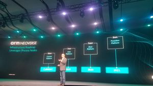
Ares was first announced by Drew Henry, Arm’s SVP and GM of Infrastructure Business Unit, at his TechCon 2018 keynote. Ares was officially unveiled on February 20, 2019.
Release Dates
Ares was officially disclosed on February 20, 2019.
Process Technology
Ares specifically takes advantage of the power and area advantages of the 7 nm process.
Architecture
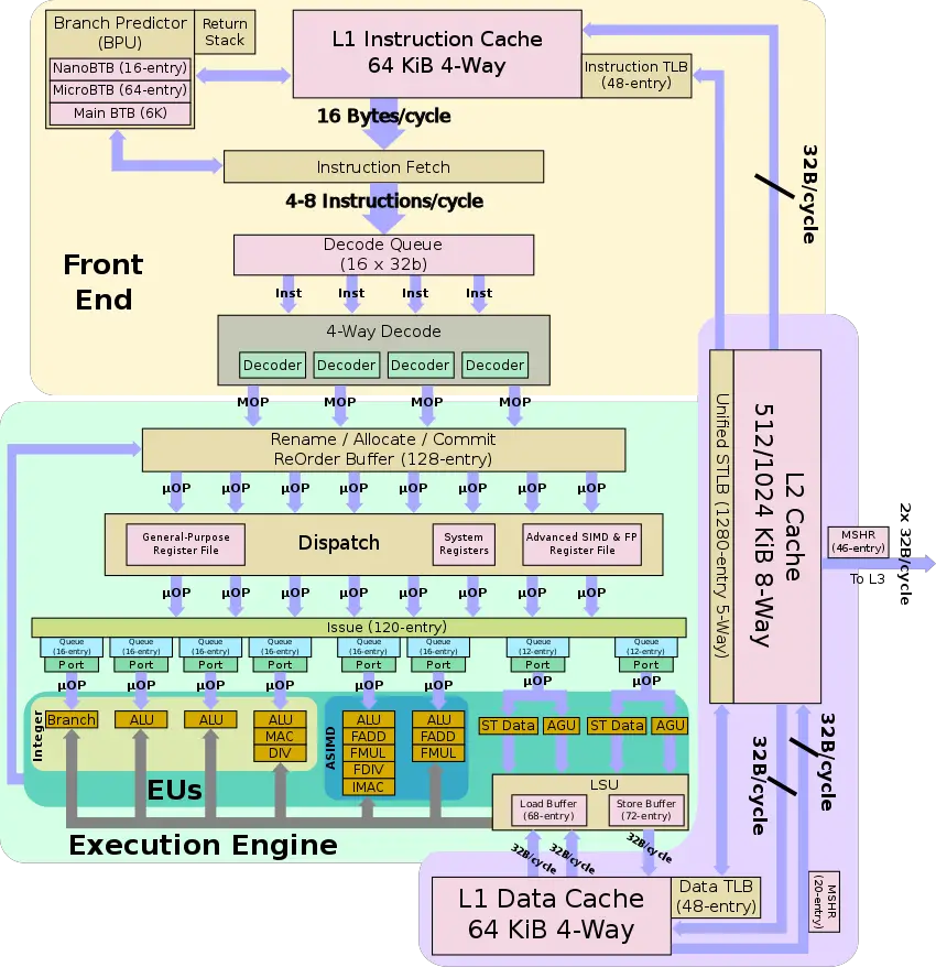
The Neoverse N1 core is almost identical to the Cortex-A76 but features a number of enhancements for infrastructure workload.
- 7 nm process
- Core
- 11-stage
- 4-way decode
- 8-way issue
- System architecture
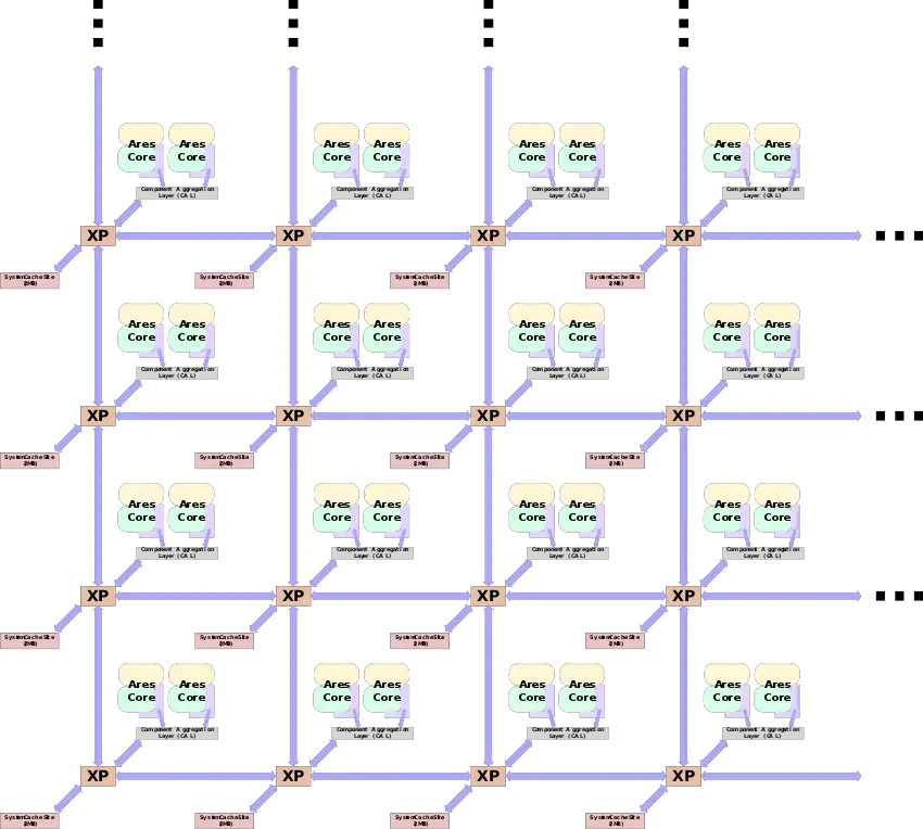
- Designed for the Coherent Mesh Network 600 (CMN-600) mesh interconnect
Block Diagram
Typical SoC
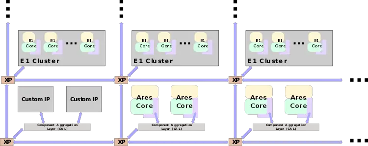
The Neoverse N1 is also expected to be integrated along with Neoverse E1 high-efficiency cores and possibly other custom IP blocks.
Individual Core
Memory Hierarchy
The Neoverse N1 has a private L1I, L1D, and L2 cache.
- Cache
- L1I Cache
- 64 KiB, 4-way set associative
- 64-byte cache lines
- SECDED ECC
- Write-back
- L1D Cache
- 64 KiB, 4-way set associative
- 64-byte cache lines
- 4-cycle fastest load-to-use latency
- SECDED ECC
- Write-back
- L2 Cache
- 512 KiB OR 1 MiB (2 banks)
- 8-way set associative
- 9-11 cycle
- 9-cycle fastest load-to-use latency
- ECC protection per 64 bits
- Modified Exclusive Shared Invalid (MESI) coherency
- Strictly inclusive of the L1 data cache & non-inclusive of the L1 instruction cache
- Write-back
- System-level cache (SLC)
- 1 Bank per core duplex
- 2 MiB to 4 MiB, 16-way set associative
- L1I Cache
The Neoverse N1 TLB consists of dedicated L1 TLB for instruction cache (ITLB) and another one for data cache (DTLB). Additionally, there is a unified L2 TLB (STLB).
- TLBs
- ITLB
- 4 KiB, 16 KiB, 64 KiB, 2 MiB, and 32 MiB page sizes
- 48-entry fully associative
- DTLB
- 48-entry fully associative
- 4 KiB, 16 KiB, 64 KiB, 2 MiB, and 512 MiB page sizes
- STLB
- 1280-entry 5-way set associative
- ITLB
Overview
| This section is empty; you can help add the missing info by editing this page. |
Core
| This section is empty; you can help add the missing info by editing this page. |
Die
N1 core
- 7 nm process
- 1 Core + L2
- 1.2 mm² die size (1C + 512 KiB L2)
- 1.4 mm² die size (1C + 1 MiB L2)
- 1 W @ 2.6 GHz (0.75 V), 1.8 W @ 3.1 W (1.0 V)
All Neoverse N1 Processors
| List of Neoverse N1-based Processors | ||||||||
|---|---|---|---|---|---|---|---|---|
| Model | Family | Launched | Process | Arch | Cores | Frequency | ||
| ALC12B00 | Graviton | 3 December 2019 | 7 nm 0.007 μm 7.0e-6 mm | Neoverse N1 | 64 | 2.5 GHz 2,500 MHz 2,500,000 kHz | ||
| Count: 1 | ||||||||
Bibliography
- Drew Henry keynote, TechCon 2018 keynote.
- Drew Henry, direct communication
- Most of the technical details were obtained directly from Arm
| codename | Ares + |
| core count | 4 +, 8 +, 16 +, 32 +, 64 +, 96 + and 128 + |
| designer | ARM Holdings + |
| first launched | February 20, 2019 + |
| full page name | arm holdings/microarchitectures/neoverse n1 + |
| instance of | microarchitecture + |
| instruction set architecture | ARMv8.2 + |
| manufacturer | TSMC + |
| microarchitecture type | CPU + |
| name | Ares + |
| pipeline stages | 11 + |
| process | 7 nm (0.007 μm, 7.0e-6 mm) + |
