(fixed) |
|||
| Line 1: | Line 1: | ||
{{amd title|Package ASB2}} | {{amd title|Package ASB2}} | ||
{{package | {{package | ||
| − | |name=ASB2 | + | |name=Package ASB2 |
|designer=AMD | |designer=AMD | ||
|market=Mobile | |market=Mobile | ||
| Line 8: | Line 8: | ||
|tdp=15 W | |tdp=15 W | ||
|package name=ASB2 | |package name=ASB2 | ||
| + | |package name 2=BGA-812 | ||
|package type=Organic Micro Ball Grid Array | |package type=Organic Micro Ball Grid Array | ||
|package contacts=812 | |package contacts=812 | ||
| Line 15: | Line 16: | ||
}} | }} | ||
| − | '''ASB2''' was a BGA-812 package for low power [[AMD]] mobile microprocessors with an | + | '''Package ASB2''' was a BGA-812 package for low power [[AMD]] mobile microprocessors with an |
| − | integrated DDR3 memory controller targeting the small form factor desktop, mobile and embedded market. | + | integrated DDR3 memory controller targeting the small form factor desktop, mobile and embedded market. |
| − | ASB2 was the successor to the {{\\|ASB1}} package. Its counterparts for the mainstream mobile and desktop markets are | + | ASB2 was the successor to the {{\\|ASB1}} package. Its counterparts for the mainstream mobile and desktop |
| − | {{\\|Socket S1g4}} and {{\\|Socket AM3}}. ASB2 was superseded by the {{\\|FT1}} package. | + | markets are {{\\|Socket S1g4}} and {{\\|Socket AM3}}. ASB2 was superseded by the {{\\|FT1}} package. |
Package ASB2 was used in AMD's "Nile" platform for ultrathin notebooks. | Package ASB2 was used in AMD's "Nile" platform for ultrathin notebooks. | ||
All ASB2 processors belong to AMD's Family 10h based on the [[amd/microarchitectures/k10|K10 microarchitecture]], | All ASB2 processors belong to AMD's Family 10h based on the [[amd/microarchitectures/k10|K10 microarchitecture]], | ||
| − | codename "Geneva", and were manufactured in a 45 nm SOI process. | + | codename "Geneva", and were manufactured in a [[45 nm]] SOI process. |
Package ASB1 and ASB2 appear to have the same dimensions but are electrically incompatible. | Package ASB1 and ASB2 appear to have the same dimensions but are electrically incompatible. | ||
=== Features === | === Features === | ||
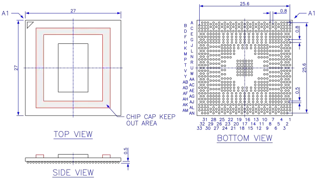
| − | * 812-pin lidless micro ball grid array package, 0.8-1.6 mm multi-pitch, 33 × 33 pins, 27 × 27 mm, organic substrate | + | * 812-pin lidless micro ball grid array package, 0.8 - 1.6 mm multi-pitch, 33 × 33 pins, 27 × 27 mm, organic substrate |
| − | * 16 bit | + | * 16 bit HyperTransport 3.0 interface up to 1.6 GHz, 3200 MT/s, 6.8 Gbyte/s in each direction |
* 2 × 64/72 bit DDR3 SDRAM interface (unganged only) up to 533 MHz, PC3-8500 (DDR3-1066), 17.0 Gbyte/s | * 2 × 64/72 bit DDR3 SDRAM interface (unganged only) up to 533 MHz, PC3-8500 (DDR3-1066), 17.0 Gbyte/s | ||
** Up to 2 SODIMMs, SEC-DED ECC | ** Up to 2 SODIMMs, SEC-DED ECC | ||
Latest revision as of 14:23, 7 October 2025
| Edit Values | |
| Package ASB2 | |
| General Info | |
| Designer | AMD |
| Introduction | May 12, 2010 (launched) |
| Market | Mobile |
| Microarchitecture | K10 |
| TDP | 15 W 15,000 mW 0.0201 hp 0.015 kW |
| Package | |
| Name | ASB2, BGA-812 |
| Type | Organic Micro Ball Grid Array |
| Contacts | 812 |
| Dimension | 27 mm 2.7 cm × 27 mm1.063 in 2.7 cm 1.063 in |
| Pitch | 0.8 mm 0.0315 in |
Package ASB2 was a BGA-812 package for low power AMD mobile microprocessors with an integrated DDR3 memory controller targeting the small form factor desktop, mobile and embedded market. ASB2 was the successor to the ASB1 package. Its counterparts for the mainstream mobile and desktop markets are Socket S1g4 and Socket AM3. ASB2 was superseded by the FT1 package.
Package ASB2 was used in AMD's "Nile" platform for ultrathin notebooks. All ASB2 processors belong to AMD's Family 10h based on the K10 microarchitecture, codename "Geneva", and were manufactured in a 45 nm SOI process.
Package ASB1 and ASB2 appear to have the same dimensions but are electrically incompatible.
Contents
Features[edit]
- 812-pin lidless micro ball grid array package, 0.8 - 1.6 mm multi-pitch, 33 × 33 pins, 27 × 27 mm, organic substrate
- 16 bit HyperTransport 3.0 interface up to 1.6 GHz, 3200 MT/s, 6.8 Gbyte/s in each direction
- 2 × 64/72 bit DDR3 SDRAM interface (unganged only) up to 533 MHz, PC3-8500 (DDR3-1066), 17.0 Gbyte/s
- Up to 2 SODIMMs, SEC-DED ECC
- JEDEC 1.35V (DDR3L), 1.5V
- Core and NB P-States; ACPI C0, C1, C1E, S0, S1, S3, S4, S5; Separate core and NB power planes
- Thermal diode, overtemperature protection
Chipsets[edit]
- AMD RS880M
Processors using package ASB2[edit]
- AMD Turion II Neo Dual-Core
- AMD Athlon II Neo Dual-Core
- AMD Athlon II Neo
- AMD V-Series Dual-Core
- AMD V-Series
| List of all ASB2-based Processors | |||||||||||||||||||
|---|---|---|---|---|---|---|---|---|---|---|---|---|---|---|---|---|---|---|---|
| Model | Price | Process | Launched | µarch | Family | Core | C | T | Freq | Turbo | TDP | ||||||||
| Count: 0 | |||||||||||||||||||
Package Diagram[edit]
No data available. Approximate dimensions of the Athlon II Neo package. All dimensions in millimeters.
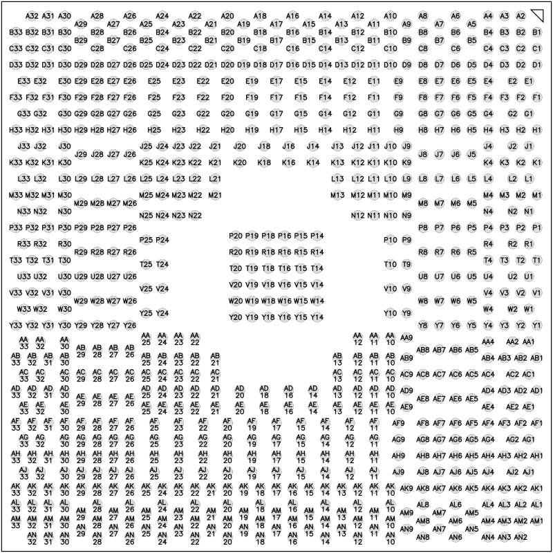
BGA-812 package pin (ball) numbering.
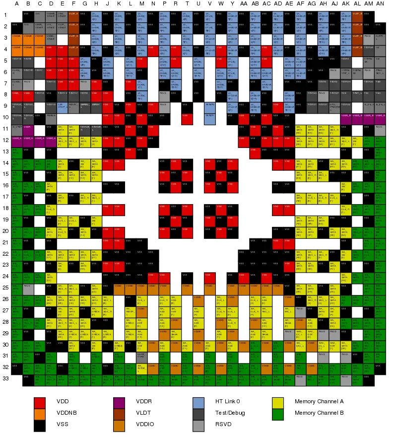
Pin Map[edit]
References[edit]
- "BIOS and Kernel Developer’s Guide (BKDG) for AMD Family 10h Processors", AMD Publ. #31116, Rev. 3.48, April 22, 2010
- "Revision Guide for AMD Family 10h Processors", AMD Publ. #41322, Rev. 3.92, March 2012
- The 2010 AMD Ultrathin Platform, amd.com, archived May 2010
See also[edit]
| designer | AMD + |
| first launched | May 12, 2010 + |
| instance of | package + |
| market segment | Mobile + |
| microarchitecture | K10 + |
| name | Package ASB2 + |
| package | ASB2 + and BGA-812 + |
| package contacts | 812 + |
| package length | 27 mm (2.7 cm, 1.063 in) + |
| package pitch | 0.8 mm (0.0315 in) + |
| package type | Organic Micro Ball Grid Array + |
| package width | 27 mm (2.7 cm, 1.063 in) + |
| tdp | 15 W (15,000 mW, 0.0201 hp, 0.015 kW) + |


