(→New instructions) |
(→Die) |
||
| Line 165: | Line 165: | ||
:[[File:ice lake die core (annotated).png|400px]] | :[[File:ice lake die core (annotated).png|400px]] | ||
| + | |||
| + | |||
| + | :[[File:ice lake die core 2.png|500px]] | ||
=== Core group === | === Core group === | ||
| Line 177: | Line 180: | ||
:[[File:ice lake die core group (annotated).png|700px]] | :[[File:ice lake die core group (annotated).png|700px]] | ||
| + | |||
| + | |||
| + | :[[File:ice lake die core group 2.png|800px]] | ||
== Bibliography == | == Bibliography == | ||
* Intel Architecture Day 2018, December 11, 2018 | * Intel Architecture Day 2018, December 11, 2018 | ||
Revision as of 21:42, 29 May 2019
| Edit Values | |
| Sunny Cove µarch | |
| General Info | |
| Arch Type | CPU |
| Designer | Intel |
| Manufacturer | Intel |
| Introduction | 2019 |
| Process | 10 nm |
| Core Configs | 2, 4 |
| Pipeline | |
| Type | Superscalar |
| OoOE | Yes |
| Speculative | Yes |
| Reg Renaming | Yes |
| Stages | 14-19 |
| Instructions | |
| ISA | x86-64 |
| Extensions | MOVBE, MMX, SSE, SSE2, SSE3, SSSE3, SSE4.1, SSE4.2, POPCNT, AVX, AVX2, AES, PCLMUL, FSGSBASE, RDRND, FMA3, F16C, BMI, BMI2, VT-x, VT-d, TXT, TSX, RDSEED, ADCX, PREFETCHW, CLFLUSHOPT, XSAVE, SGX, MPX, AVX-512 |
| Cache | |
| L1I Cache | 32 KiB/core 8-way set associative |
| L1D Cache | 48 KiB/core 12-way set associative |
| L2 Cache | 512 KiB/core 8-way set associative |
| L3 Cache | 2 MiB/core 16-way set associative |
| Succession | |
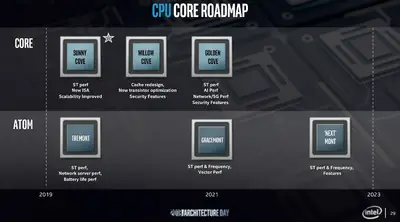
Sunny Cove is the successor to Palm Cove, a high-performance 10 nm x86 core microarchitecture designed by Intel for an array of server and client products, including Ice Lake (Client), Ice Lake (Server), Lakefield, and the Nervana NNP-I. The microarchitecture was developed by Intel's R&D Center (IDC) in Haifa, Israel.
Contents
History
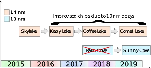
Sunny Cove was originally unveiled by Intel at their 2018 architecture day. Intel originally intended for Sunny Cove to succeed Palm Cove in late 2017 which was it was intended to be the first 10 nm-based core and the proper successor to Skylake. Prolong delays and problems with their 10 nm process and resulted in a number of improvised derivatives of Skylake including Kaby Lake, Coffee Lake, and Comet Lake. For all practical purposes, Palm Cove has been skipped and Intel has gone directly to Sunny Cove. Sunny Cove is expected to debut in mid-2019.
Process Technology
Sunny Cove is designed to take advantage of Intel's 10 nm process.
Architecture
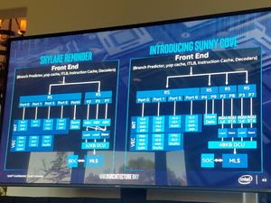
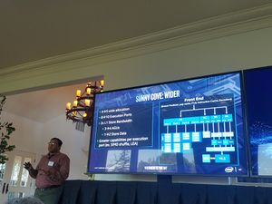
Key changes from Palm Cove/Skylake
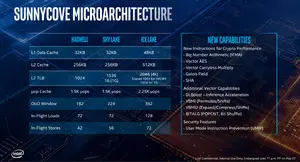
- Significant IPC uplift (Intel self-reported average 18% IPC accross proxy benchmarks such as SPEC CPU2006/SPEC CPU2017)
- Front-end
- 1.5x larger µOP cache (2.25k entries, up from 1536)
- Back-end
- Wider allocation (5-way, up from 4-way)
- 1.6x larger ROB (352, up from 224 entries)
- Scheduler
- Larger scheduler (?, up from 97 entries)
- Larger dispatch (10-way, up from 8-way)
- Execution ports rebalanced
- New store data port
- New store AGU port
- Memory subsystem
- LSU
- 1.8x more inflight loads (128, up from 72 entries)
- 1.7x more inflight stores (72, up from 42 entries)
- Larger L1 data cache (48 KiB, up from 32 KiB)
- Larger L2 cache (512 KiB, up from 256 KiB)
- Larger STLBs
- Larger 1G table (1024-entry, up from 16)
- Larger 4k table (2048 entries, up from 1536)
- New 1,024-entry 2M/4M table
- Larger STLBs
- 5-Level Paging
- Large virtual address (57 bits, up from 48 bits)
- Significantly large virtual address space (128 PiB, up from 256 TiB)
- LSU
This list is incomplete; you can help by expanding it.
New instructions
Sunny Cove introduced a number of new instructions:
-
SHA- Hardware acceleration for SHA hashing operations -
CLWB- Force cache line write-back without flush -
RDPID- Read Processor ID - Additional AVX-512 extensions:
-
AVX512VPOPCNTDQ- AVX-512 Vector Population Count Doubleword and Quadword -
AVX512VNNI- AVX-512 Vector Neural Network Instructions -
AVX512GFNI- AVX-512 Galois Field New Instructions -
AVX512VAES- AVX-512 Vector AES -
AVX512VBMI2- AVX-512 Vector Bit Manipulation, Version 2 -
AVX512BITALG- AVX-512 Bit Algorithms -
AVX512VPCLMULQDQ- AVX-512 Vector Vector Carry-less Multiply
-
-
SSE_GFNI- SSE-based Galois Field New Instructions -
AVX_GFNI- AVX-based Galois Field New Instructions - Split Lock Detection - detection and cause an exception for split locks
- Fast Short REP MOV
Only on server parts (Ice Lake (Server)):
-
TME- Total Memory Encryption -
PCONFIGPlatform Configuration -
WBNOINVDWrite-back and do not invalidate cache -
ENCLV- SGX oversubscription instructions
Block diagram
Overview
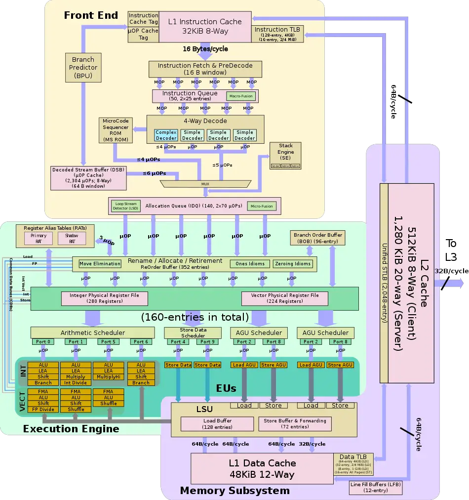
Sunny Cove is Intel's microarchitecture for the CPU core which is incorporated into a number of client and server chips that succeed Palm Cove (and effectively the Skylake series of derivatives). Sunny Cove is just the core which is implemented in a numerous chips made by Intel including Lakefield, Ice Lake (Client), Ice Lake (Server), and the Nervana NNP accelerator. Sunny Cove introduces a large set of enhancements that significantly improves the performance of legacy code and new code through the extraction of parallelism as well as new features. Those include a significantly deep out-of-window pipeline, a wider execution back-end, higher load-store bandwidth, lower effective access latencies, and bigger caches.
Pipeline
Like it's predecessors, Sunny Cove focuses on extracting performance and reducing power through a number of key ways. Intel builds Sunny Cove on previous microarchitectures, descendants of Sandy Bridge. For the core to increase the overall performance, Intel focused on extracting additional parallelism.
Broad Overview
At a 5,000 foot view, Sunny Cove represents the logical evolution from Skylake and Haswell. Therefore, despite some significant differences from the previous microarchitecture, the overall designs is fundamentally the same and can be seen as enhancements over Skylake rather than a complete change.
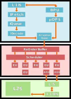
The pipeline can be broken down into three areas: the front-end, back-end or execution engine, and the memory subsystem. The goal of the front-end is to feed the back-end with a sufficient stream of operations which it gets by decoding instructions coming from memory. The front-end has two major pathways: the µOPs cache path and the legacy path. The legacy path is the traditional path whereby variable-length x86 instructions are fetched from the level 1 instruction cache, queued, and consequently get decoded into simpler, fixed-length µOPs. The alternative and much more desired path is the µOPs cache path whereby a cache containing already decoded µOPs receives a hit allowing the µOPs to be sent directly to the decode queue.
Regardless of which path an instruction ends up taking it will eventually arrive at the decode queue. The IDQ represents the end of the front-end and the in-order part of the machine and the start of the execution engine which operates out-of-order.
In the back-end, the micro-operations visit the reorder buffer. It's there where register allocation, renaming, and retiring takes place. At this stage a number of other optimizations are also done. From the reorder buffer, µOPs are sent to the unified scheduler. The scheduler has a number of exit ports, each wired to a set of different execution units. Some units can perform basic ALU operations, others can do multiplication and division, with some units capable of more complex operations such as various vector operations. The scheduler is effectively in charge of queuing the µOPs on the appropriate port so they can be executed by the appropriate unit.
Some µOPs deal with memory access (e.g. load & store). Those will be sent on dedicated scheduler ports that can perform those memory operations. Store operations go to the store buffer which is also capable of performing forwarding when needed. Likewise, Load operations come from the load buffer. Sunny Cove features a dedicated 48 KiB level 1 data cache and a dedicated 32 KiB level 1 instruction cache. It also features a core-private 512 KiB L2 cache that is shared by both of the L1 caches.
Each core enjoys a slice of a third level of cache that is shared by all the core. For Ice Lake (Client) which incorporates Sunny Cove cores, there are either two cores or four cores connected together on a single chip.
Die
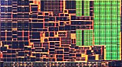
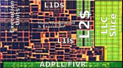
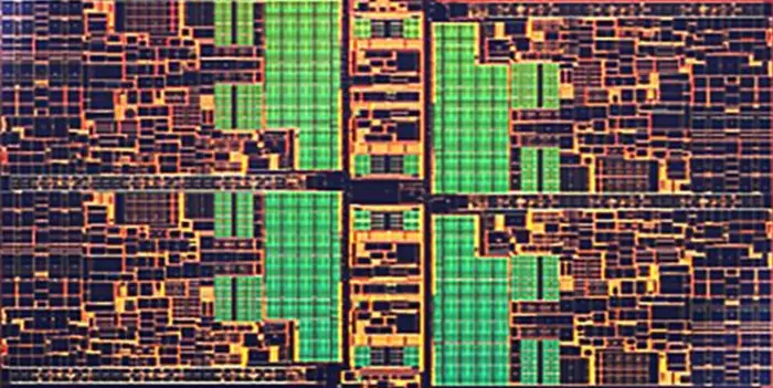
Core
- 10nm+ process
- Core from an Ice Lake SoC
- ~6.91 mm² die size
- ~3.5 mm x ~1.97 mm
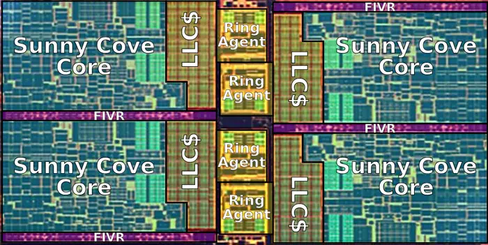
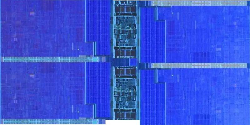
Core group
- 10nm+ process
- Quad-core from an Ice Lake SoC
- ~30.73 mm² die size
- ~7.86 mm x ~3.91 mm
Bibliography
- Intel Architecture Day 2018, December 11, 2018
| codename | Sunny Cove + |
| core count | 2 + and 4 + |
| designer | Intel + |
| first launched | 2019 + |
| full page name | intel/microarchitectures/sunny cove + |
| instance of | microarchitecture + |
| instruction set architecture | x86-64 + |
| manufacturer | Intel + |
| microarchitecture type | CPU + |
| name | Sunny Cove + |
| pipeline stages (max) | 19 + |
| pipeline stages (min) | 14 + |
| process | 10 nm (0.01 μm, 1.0e-5 mm) + |
