| Line 26: | Line 26: | ||
|package name 1=tesla_car,fcbga_2116 | |package name 1=tesla_car,fcbga_2116 | ||
}} | }} | ||
| − | '''Full Self-Driving Chip''' ('''FSD Chip''', previously '''Autopilot Hardware 3.0''') is an [[autonomous driving chip]] designed by [[tesla car|Tesla]] and announced and introduced in early [[2019]]. Fabricated on [[Samsung]]'s [[14 nm process technology]], this chip meets AEC-Q100 automotive quality standards. | + | '''Full Self-Driving Chip''' ('''FSD Chip''', previously '''Autopilot Hardware 3.0''') is an [[autonomous driving chip]] designed by [[tesla car|Tesla]] and announced and introduced in early [[2019]]. Fabricated on [[Samsung]]'s [[14 nm process technology]], this chip meets AEC-Q100 automotive quality standards. The FSD Chip incorporates 3 quad-core {{armh|Cortex-A72|l=arch}} clusters for a total of 12 CPUs operating at 2.2 GHz, a GPU operating 1 GHz, 2 [[neural processing units]] operating at 2 GHz, and various other hardware accelerators. The FSD supports up to octa-channel LPDDR4-4266 memory. |
== History == | == History == | ||
Revision as of 16:18, 26 April 2019
| Edit Values | |
| FSD Chip | |
 | |
| General Info | |
| Designer | Tesla (car company) |
| Manufacturer | Samsung |
| Market | Automotive |
| Introduction | April 22, 2019 (announced) March 10, 2019 (launched) |
| General Specs | |
| Frequency | 2,200 MHz |
| Microarchitecture | |
| ISA | ARMv8.0-A (ARM) |
| Microarchitecture | Cortex-A72 |
| Core Name | Cortex-A72 |
| Core Stepping | B0 |
| Process | 14 nm |
| Transistors | 6,000,000,000 |
| Technology | CMOS |
| Die | 260 mm² 20 mm × 13 mm |
| Word Size | 64 bit |
| Cores | 12 |
| Threads | 12 |
| Packaging | |
| Package | FCBGA-2116 (BGA) |
| Dimension | 37.5 mm × 37.5 mm |
| Contacts | 2116 |
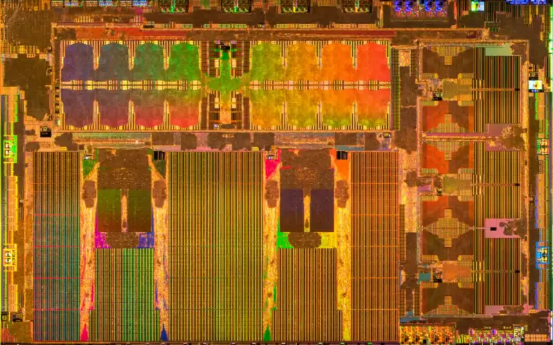
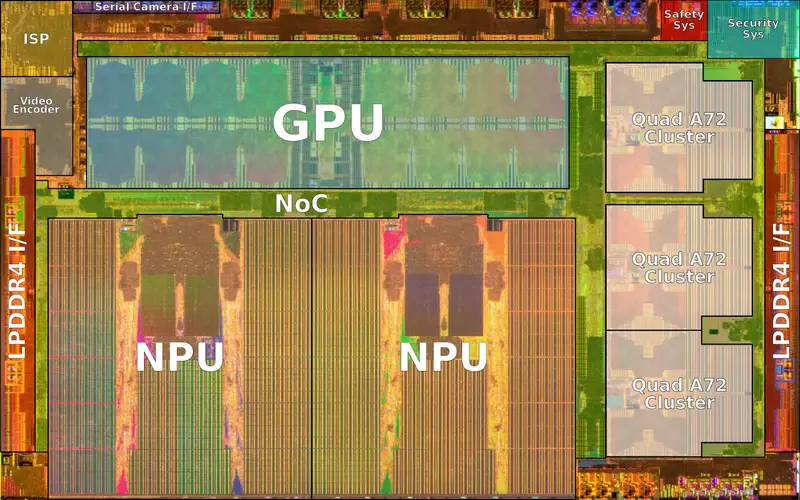
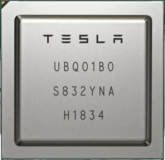
Full Self-Driving Chip (FSD Chip, previously Autopilot Hardware 3.0) is an autonomous driving chip designed by Tesla and announced and introduced in early 2019. Fabricated on Samsung's 14 nm process technology, this chip meets AEC-Q100 automotive quality standards. The FSD Chip incorporates 3 quad-core Cortex-A72 clusters for a total of 12 CPUs operating at 2.2 GHz, a GPU operating 1 GHz, 2 neural processing units operating at 2 GHz, and various other hardware accelerators. The FSD supports up to octa-channel LPDDR4-4266 memory.
Contents
History
Design and planning for the FSD chip started in 2016 when Tesla claims they saw no alternative solution that fits their problem of addressing autonomous driving. The FSD chip project was led by Pete Bannon. The design team was formed in February 2016. Development was done over the course of 18 months. In August 2017, the chip was released for manufacturing with first silicon coming back in December 2017 fully working. A number of additional modifications were done to the design, requiring respinning. B0 stepping was released to manufacturing in April 2018. Full production of B0 started shortly after qualifications in July 2018. In December 2018, Tesla started retrofitting employee cars with the new hardware and software stack. In March 2019, Tesla began volume shipping the FSD chip and computer in their Model S and Model X cars. Production shipment in the Tesla Model 3 started in April 2019.
Overview
| This section is empty; you can help add the missing info by editing this page. |
Full self-driving computer (FSD Computer)
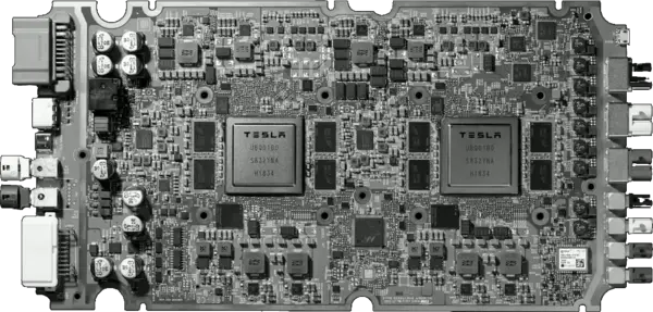
The FSD computer is designed to be retrofitted into existing Tesla models and is therefore largely the same in terms of form factor and I/O. The computer itself fits just behind the glove compartment of the car. The FSD Computer can be installed by a technician in the same slot as the prior Autopilot Hardware 2.5 board. The board itself incorporates two fully independent FSD chips along with their own power subsystem, DRAM, and flash memory for full redundancy. Each chip boots up from its own storage memory and runs its own independent operating system. On the right of the board (shown below) are the eight camera connectors. The power supply and controls are on the left side of the board. The board sits on two independent power supplies - one for one of the FSD chips and one for the other. Additionally, half of the cameras sit on one power supply and the other half sit on the second power supply (note that the video input itself is received by both chips).
The computer itself intakes inputs from a variety of sources including current car readings such as acceleration and speed, radar, GPS, IMU, ultrasonic sensors, wheel ticks, steering angle, and maps data. Data is fed to both FSD chips simultaneously for processing. The two chips independently form a future plan for the car which is then consequently compared between the two chips to ensure an agreement was reached. Once the two plans from both chips agree on the calculated plan, the car can proceed and drive. The drive commands are then validated and sensory information is used as feedback for ensuring the commands executed the desired operations.
Die
SoC
- Samsung 14 nm process
- 12 metal layers
- 260 mm² die size
- ~20 mm x 13 mm die size
- 6,000,000,000 transistors
- 250,000,000 gates
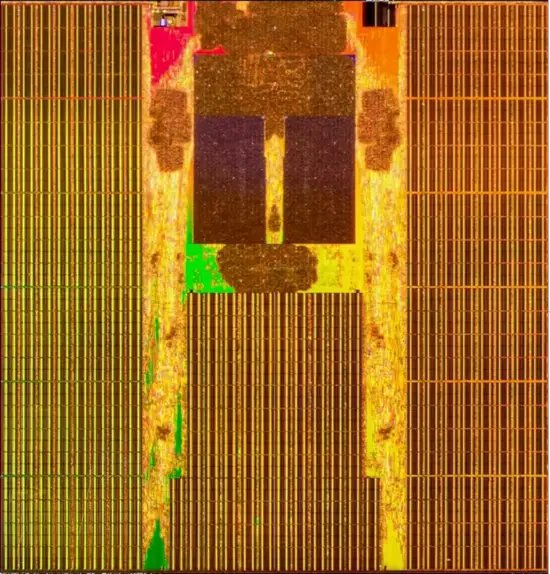
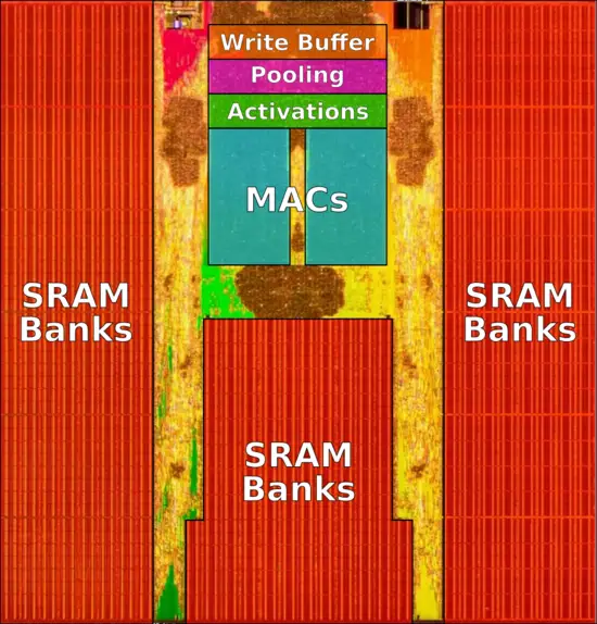
NPU
- 96 x 96 multiply-accumulates
- 9,216 MACs
- 36.864 trillion OPs
- 9,216 MACs @ 2 GHz
Top bumps
- Samsung 14 nm process
- 12 metal layers
- 12,464 C4 bumps
See also
- Nvidia Tegra Xavier
- Mobileye EyeQ
Bibliography
- Tesla Autonomy Day, Apr 22, 2019
- Tesla, personal communication, April 25, 2019
| base frequency | 2,200 MHz (2.2 GHz, 2,200,000 kHz) + |
| core count | 12 + |
| core name | Cortex-A72 + |
| core stepping | B0 + |
| designer | Tesla (car company) + |
| die area | 260 mm² (0.403 in², 2.6 cm², 260,000,000 µm²) + |
| die length | 20 mm (2 cm, 0.787 in, 20,000 µm) + |
| die width | 13 mm (1.3 cm, 0.512 in, 13,000 µm) + |
| first announced | April 22, 2019 + |
| first launched | March 10, 2019 + |
| full page name | tesla (car company)/fsd chip + |
| instance of | microprocessor + |
| isa | ARMv8.0-A + |
| isa family | ARM + |
| ldate | March 10, 2019 + |
| main image |  + + |
| manufacturer | Samsung + |
| market segment | Automotive + |
| microarchitecture | Cortex-A72 + |
| name | FSD Chip + |
| package | FCBGA-2116 + |
| process | 14 nm (0.014 μm, 1.4e-5 mm) + |
| technology | CMOS + |
| thread count | 12 + |
| transistor count | 6,000,000,000 + |
| word size | 64 bit (8 octets, 16 nibbles) + |
