| Line 23: | Line 23: | ||
|successor=ARM6 | |successor=ARM6 | ||
|successor link=arm holdings/microarchitectures/arm6 | |successor link=arm holdings/microarchitectures/arm6 | ||
| − | |||
| − | |||
}} | }} | ||
'''ARM3''' is the second-generation commercial [[ARM]] implementation designed by [[Acorn Computers]] as a successor to the {{\\|ARM2}}. | '''ARM3''' is the second-generation commercial [[ARM]] implementation designed by [[Acorn Computers]] as a successor to the {{\\|ARM2}}. | ||
Revision as of 17:14, 10 July 2017
| Edit Values | |
| ARM3 µarch | |
| General Info | |
| Arch Type | CPU |
| Designer | Acorn Computers |
| Manufacturer | VLSI Technology, Sanyo |
| Introduction | 1989 |
| Process | 1.5 µm |
| Core Configs | 1 |
| Pipeline | |
| Type | Scalar, Pipelined |
| Stages | 3 |
| Decode | 1-way |
| Instructions | |
| ISA | ARMv2a |
| Cache | |
| L1 Cache | 4 KiB/core 64-way set associative |
| Cores | |
| Core Names | ARM3, ARM250 |
| Succession | |
ARM3 is the second-generation commercial ARM implementation designed by Acorn Computers as a successor to the ARM2.
Contents
History
- See also: ARM's History
The ARM3 builds on the success of the ARM2 with higher performance through the introduction of on-die cache but without any major changes to the core itself. The ARM3 was designed by a team of four engineers in nine months and was introduced in 1989. The ARM3 can operate at up to 25 MHz with a peak performance of 25 MIPS and a sustainable performance of 12 MIPS.
Process Technology
- See also: 1.5 µm process
The ARM3 was implemented on a 1.5 µm double-level metal (DLM) CMOS process.
Architecture
The major goal of the ARM3 was to improve performance. A target of three times the performance of the ARM2 was set. In order to support a faster microprocessor, the system would have to use faster DRAM which would negatively impact the overall cost. Instead, the design team opted to integrating cache.
Key changes from ARM2
- Goal 3x the performance
- Integrated cache
- Integrated clock generator
- Integrated control logic
- Integrated co-processor interface
New instructions
New ARM3 instructions:
Memory:
-
SWP- Swap word memory-register, Atomic (uninterruptible)
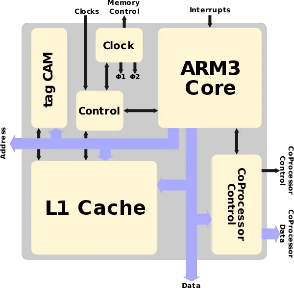
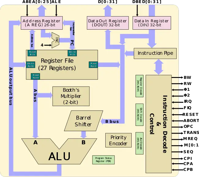
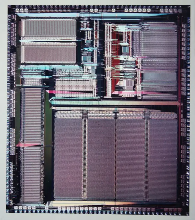
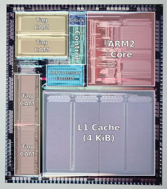
Block Diagram
Entire Chip
Core
Memory Hierarchy
- Cache
- L1 Cache (unified)
- 4 KiB, 64-way set associative
- 16 B line size
- Write-through policy
- Per core
- L1 Cache (unified)
- System DRAM
- Up to 64 MiB
Overview
Control
The ARM3's control logic is a state machine implemented as three PLAs. Layout was generated automatically using EDA tools using Psuedo nMOS logic in order to save on space, albeit at the slight expense of static power dissipation.
Core
Pipeline
- Main article: ARM2 Pipeline
ARM3's pipeline is identical to the ARM2.
Clock Generator
To increase performance, Acorn needed to increase the clock speed. This was not possible without leaving commodity DRAM for higher speed and more expensive DRAM. The alternative approach Acorn went with is an intermediate cache on-die. The ARM3 has two clock inputs, one fast one for the internal cache and one slower one for the external memory accesses. The two inputs are entirely independent allowing the system to optimize for both (fast cache and slower memory) at the same time.
Coprocessor Interface
Acorn introduced cache with the ARM3. This meant that most instructions are now coming from the on-chip cache instead of system memory. The way the coprocessor was originally designed in the ARM2 meant that the coprocessor could simply access its instructions from memory. This was no longer compatible with the new design. Acorn solved this problem by making the coprocessor lag behind exactly one cycle. Instructions that are identified as being coprocessor instructions are broadcasted off-chip on the following cycle. This was done using the processor's 32-bit data port along with timing and handshaking signals.
Cache
The ARM3's cache consists of a RAM and 4 tag CAM banks of 64 22-bit entries each for 64-way set associative. The choice of a 4-way split was entirely driven by the great reduction in power dissipation, at the cost of negligible performance (due to only 1/4th of the total CAM being enabled at any given time). Each CAM entry refers to one line of data in the RAM. Each line consists of four 32-bit words (i.e., 128 bit lines) with the low-order address bits being used for the select lines.
On a miss, a pseudo-random number generator is used to select an entry to evict and replace. On replacement a full line of four words is fetched from memory to minimize consecutive read operations. The cache uses a write-through update policy to ensure consistency. On a hit the appropriate line address are generated to be retrieved by the RAM.
The CAM consists of individual cells of six-transistor storage elements with a three-transistor comparators. The cell size was reported by Acorn to be 31.2 µm x 36.8 µm (1148.16 µm²) on a 1.5 µm process. The entry matching and address encoding logic uses dynamic logic in order to reduce power. The RAM is arranged in array of 128 x 256 cells with a 3-bit column elect, producing a 32-bit output. The SRAM cells used were standard 6T SRAM cells measuring 19.6 µm x 28.4 µm. Self-timing logic is used to disable the 32 sense amplifiers when the data becomes valid in order to reduce power.
Die
- 12 MHz, 1 W
- 1.5 µm DLM CMOS
- 8.72 mm x 9.95 mm
- 86.764 mm² die size
- 309,656 transistors
- 206,454 SRAM
- 62,973 CAM
- 40,229 logic
- QFP-160
- 119 signal pins
- 41 power/ground pins
All ARM3 Chips
| List of ARM3-based Processors | ||||||||||||
|---|---|---|---|---|---|---|---|---|---|---|---|---|
| Model | Process | Launched | Frequency | Power Dissipation | Max Memory | |||||||
| VL86C020 | ARM3 | 1989 | 20 MHz 0.02 GHz , 25 MHz20,000 kHz 0.025 GHz , 33 MHz25,000 kHz 0.033 GHz , 36 MHz33,000 kHz 0.036 GHz 36,000 kHz | 2 W 2,000 mW 0.00268 hp 0.002 kW | 64 MiB 65,536 KiB 67,108,864 B 0.0625 GiB 6.103516e-5 TiB | |||||||
| Count: 1 | ||||||||||||
References
- Thomas, A. R. P., et al. "A 2nd Generation 32b RISC Processor with 4KByte Cache." Solid-State Circuits Conference, 1989. ESSCIRC'89. Proceedings of the 15th European. IEEE, 1989.
| codename | ARM3 + |
| core count | 1 + |
| designer | Acorn Computers + |
| first launched | 1989 + |
| full page name | acorn/microarchitectures/arm3 + |
| instance of | microarchitecture + |
| instruction set architecture | ARMv2a + |
| manufacturer | VLSI Technology + and Sanyo + |
| microarchitecture type | CPU + |
| name | ARM3 + |
| pipeline stages | 3 + |
| process | 1,500 nm (1.5 μm, 0.0015 mm) + |


