(visual) |
(→Pipeline) |
||
| Line 76: | Line 76: | ||
=== Pipeline === | === Pipeline === | ||
Much like other x86 microarchitectures, Bonnell converts the complex instructions into finer [[micro-ops]] when needed. However, most instructions in Bonnell do not break down into simpler micro-ops (since Bonnell is not OoOE, there is no real advantage in doing so anyway). Intel estimates that only 5% of common software require instructions to be split up. Bonnell has a 16-stage pipeline with a 13-stage miss penalty. Bonnell is a dual-issue [[superscalar]] but with in-order execution (in fact, first microarchitecture since {{intel|Pentium Pro}} to not feature a OoOE). The elimination of reordering logic allowed for lower power consumption and small die area. This does imply the overall MPU is less efficient in managing its own resources; memory accesses and FP operations also stall the whole pipeline. Bonnell employed [[Safe Instruction Recognition]] (SIR) and [[Simultaneous multithreading]] (SMT) to bring performance to acceptable level. Intel claimed sub-20% power consumption penalty while improving performance between 30% and 50%. | Much like other x86 microarchitectures, Bonnell converts the complex instructions into finer [[micro-ops]] when needed. However, most instructions in Bonnell do not break down into simpler micro-ops (since Bonnell is not OoOE, there is no real advantage in doing so anyway). Intel estimates that only 5% of common software require instructions to be split up. Bonnell has a 16-stage pipeline with a 13-stage miss penalty. Bonnell is a dual-issue [[superscalar]] but with in-order execution (in fact, first microarchitecture since {{intel|Pentium Pro}} to not feature a OoOE). The elimination of reordering logic allowed for lower power consumption and small die area. This does imply the overall MPU is less efficient in managing its own resources; memory accesses and FP operations also stall the whole pipeline. Bonnell employed [[Safe Instruction Recognition]] (SIR) and [[Simultaneous multithreading]] (SMT) to bring performance to acceptable level. Intel claimed sub-20% power consumption penalty while improving performance between 30% and 50%. | ||
| − | |||
:[[File:bonnell pipeline.svg]] | :[[File:bonnell pipeline.svg]] | ||
| + | The longer pipeline allows a more evenly spreading of heat across the chip with more units. This also allows a higher clock rate. | ||
* '''Instruction Fetch''' | * '''Instruction Fetch''' | ||
| Line 105: | Line 105: | ||
* '''Commit''' | * '''Commit''' | ||
** 1 stage | ** 1 stage | ||
| + | |||
| + | === Multithreading === | ||
| + | Bonnell has support for multithreading - up to two threads per core. However each thread compete for the same resources which does inherently means they run slower than they would if they were to run alone. | ||
| + | |||
| + | === Branch Prediction === | ||
| + | * [[Two-level adaptive predictor]] | ||
| + | * 12-bit branch history register | ||
| + | * Pattern history table has 4096 entries (shared between threads) | ||
| + | * Branch buffer target has 128 entries (4-way, 32 sets) | ||
| + | * Unconditional jumps are ignored | ||
| + | * Always-taken and never-taken are marked in the table | ||
| + | * Penalties: | ||
| + | ** 13 stages for miss prediction | ||
| + | ** 7 stages for correct prediction but missing [[branch target buffer]] (BTB) | ||
== Die == | == Die == | ||
Revision as of 19:27, 7 April 2016
| Edit Values | |
| Bonnell µarch | |
| General Info |
Bonnell was a microarchitecture for Intel's 45 nm ultra-low power microprocessors first introduced in 2008 for their then-new Atom family. Bonnell, which was named after the highest point in Austin - Mount Bonnell, was Intel's first x86-compatible microarchitecture designed to target the ultra-low power market.
Contents
Architecture
Bonnell's primary goals were:
- Reduce power consumption,
- while staying fully x86-compatible,
- at acceptable performance
Performance/Power new rule: +1% performance for at most +1% power consumption.
Memory Hierarchy
- Cache
- Hardware prefetchers
- L1 Cache:
- 32 KB 8-way set associative instruction
- 1 read and 1 write port
- 24 KB 6-way set associative data
- 1 read and 1 write port
- 8 transistors (instead of 6) to reduce voltage
- Per core
- 32 KB 8-way set associative instruction
- L2 Cache:
- 512 KB 8-way set associative
- ECC
- Shrinkable from 512 KB to 128 KB (2-way)
- Per core
- L3 Cache:
- No level 3 cache
- RAM
- Maximum of 2 GB, 4 GB, and 8 GB
Note that the L1 cache for data and instructions were originally both 32 KB (8-way), however due to power restrictions, the L1d$ was later reduced to 24 KB.
Functional Units
The number of functional units were kept to minimum to cut on power consumption.
- 2 Integer ALUs (1 for jumps, 1 for shifts)
- 2 FP ALUs (1 adder, 1 for others)
- No Integer multiplier & divider
Pipeline
Much like other x86 microarchitectures, Bonnell converts the complex instructions into finer micro-ops when needed. However, most instructions in Bonnell do not break down into simpler micro-ops (since Bonnell is not OoOE, there is no real advantage in doing so anyway). Intel estimates that only 5% of common software require instructions to be split up. Bonnell has a 16-stage pipeline with a 13-stage miss penalty. Bonnell is a dual-issue superscalar but with in-order execution (in fact, first microarchitecture since Pentium Pro to not feature a OoOE). The elimination of reordering logic allowed for lower power consumption and small die area. This does imply the overall MPU is less efficient in managing its own resources; memory accesses and FP operations also stall the whole pipeline. Bonnell employed Safe Instruction Recognition (SIR) and Simultaneous multithreading (SMT) to bring performance to acceptable level. Intel claimed sub-20% power consumption penalty while improving performance between 30% and 50%.
The longer pipeline allows a more evenly spreading of heat across the chip with more units. This also allows a higher clock rate.
- Instruction Fetch
- 3 stages
- 8 Bytes/Cycle (lower if SMT)
- Instruction Decode
- 3 stages
- Instructions with up to 3 prefixes/Cycle
- Instruction Dispatch
- 2 stages
- Source Operand Read
- 1 stage
- reading register operand
- 1 stage
- Data Cache Access
- 3 stages
- 1 stage for calculating
- 2 stages for reading cache
- 3 stages
- Execution
- 2 clusters
- integers
- quick cache access due to direct connection
- floating point & SIMD
- integers
- 2 clusters
- Exception & MT Handling
- 2 stages
- Commit
- 1 stage
Multithreading
Bonnell has support for multithreading - up to two threads per core. However each thread compete for the same resources which does inherently means they run slower than they would if they were to run alone.
Branch Prediction
- Two-level adaptive predictor
- 12-bit branch history register
- Pattern history table has 4096 entries (shared between threads)
- Branch buffer target has 128 entries (4-way, 32 sets)
- Unconditional jumps are ignored
- Always-taken and never-taken are marked in the table
- Penalties:
- 13 stages for miss prediction
- 7 stages for correct prediction but missing branch target buffer (BTB)
Die
 |
|

|
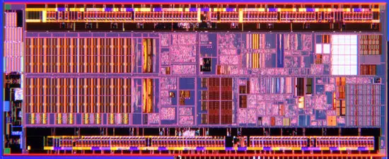
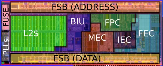
- The die is 3.1mm x 7.8mm (24.2mm2)
Cores
First generation of Bonnel-based microprocessors introduced 2 cores: Silverthorne for ultra-mobile PCs and mobile Internet devices (MIDs) and Diamondville for ultra cheap notebooks and desktops.
Silverthorne
- Main article: Silverthorne
Silverthorne was the codename for a series of ultra-mobile PCs introduced in 2008.
Key features:
- 32-bit
- 1 Core / 2 Threads
- FSB 400 MHz - 533 MHz
- Cache
- 32 KB L1i$ / 23 KB L1d$
- 512 KB L2$
- No L3$
Diamondville
- Main article: Diamondville
Diamondville was the codename for the series of ultra cheap notebooks and desktops introduced in 2008. Diamondville is very much a derivative of Silverthorne with faster FSB.
Key features:
- 32-bit
- 1 Core / 2 Threads
- FSB 533 MHz - 667 MHz
- Cache
- 32 KB L1i$ / 23 KB L1d$ (per core)
- 512 KB L2$ (per core)
- No L3$
