(Created page with "{{amd title|Socket AM5|package}} {{package |name=Socket AM5 |designer=AMD |market=Desktop |first launched= |microarch=Zen 4 |tdp=170 W |package name=AM5 |package type=FC-OLGA...") |
|||
| Line 32: | Line 32: | ||
| Type 1 | | Type 1 | ||
| {{amd|CPUID#Family 25 (19h)|Family 19h}} Models 40h–4Fh | | {{amd|CPUID#Family 25 (19h)|Family 19h}} Models 40h–4Fh | ||
| − | | {{amd|Zen | + | | <!--{{amd|Zen ?|l=arch}}--> |
| − | | <!--[[ | + | | <!--[[? nm]]--> |
| <!--Ryzen 0000 "{{amd|Codename|l=core}}" (Model 40h), Ryzen 0000 "{{amd|Codename|l=core}}" (Model 44h)--> | | <!--Ryzen 0000 "{{amd|Codename|l=core}}" (Model 40h), Ryzen 0000 "{{amd|Codename|l=core}}" (Model 44h)--> | ||
|- | |- | ||
Revision as of 15:48, 20 April 2022
| Edit Values | |
| Socket AM5 | |
| General Info | |
| Designer | AMD |
| Market | Desktop |
| Microarchitecture | Zen 4 |
| TDP | 170 W 170,000 mW 0.228 hp 0.17 kW |
| Package | |
| Name | AM5 |
| Type | FC-OLGA |
| Contacts | 1718 |
| Dimension | 40 mm 4 cm × 40 mm1.575 in 4 cm 1.575 in |
| Pitch | 0.81 mm 0.0319 in × 0.94 mm0.037 in |
| Socket | |
| Name | Socket AM5 |
| Type | SM-LGA |
| Succession | |
Socket AM5 is a microprocessor socket designed by AMD for their fifth generation Ryzen desktop processors with CPU cores based on the Zen 4 microarchitecture, the successor to Socket AM4. It has counterparts in Socket SP5 for servers and the FP7 package for the mobile market.
Contents
Overview
Socket AM5 is a zero insertion force, lever actuated, surface-mount land grid array socket for use with a 1718-contact, 0.81 mm × 0.94 mm interstitial pitch, organic land grid array CPU package.
The following AMD processor families use Socket AM5:
| x86 CPU Family | Microarch. | Process | Products | |
|---|---|---|---|---|
| Type 1 | Family 19h Models 40h–4Fh | |||
| Type 2 | Family 19h Models 60h–6Fh | |||
| Type 3 | Family 19h Models 70h–7Fh |
Socket AM5 supports two channels of DDR5 memory with two 36-bit subchannels (32 bit data + 4 bit ECC) and up to 2 DIMMs per channel, up to 28 lanes PCIe Gen 4/5, four of which are reserved to attach the chipset, four USB 3.2 Gen 2 or USB4 ports, one USB 2.0 port, and four digital display interfaces. SATA ports are provided by the chipset.
This compares to two DDR4 channels, 20 + 4 lanes PCIe Gen 3/4, four USB3 ports, and three DDIs on its predecessor Socket AM4.
Package Description
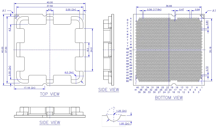
The AM5 CPU package is lidded, has a 40 mm × 40 mm organic substrate with flip chip die attachment, and 1718 land pads. The socket is not designed to be functional with unlidded packages.
The substrate has two keying notches preventing it from being inserted rotated into the socket, or incidentally into Socket F or Socket C32, two much older AMD sockets for LGA packages of the same size. Different keying options for future models are not evident, in any case AM5 packages are also electrically keyed by pin AM5R1 and Socket AM5 motherboards are not supposed to power up the socket if an incompatible processor is installed. A triangular symbol on both sides of the substrate marks the location of pin A1, with corresponding markings on the socket.
Owing to the increase of contacts from 1331 on Socket AM4 to 1718, AM5 packages have a higher contact density with the same pitch as Socket SP5, no components on the bottom side, and a redesigned lid a.k.a. integrated heat spreader which arcs over some of the top side decoupling capacitors providing more space for components.
AM5 processors are SoCs with an integrated controller hub so Socket AM5 pins out various low speed interfaces. The LPC interface present on the prior generation was deprecated in favor of SPI/ESPI. These busses are generally used to access firmware (PSP ROM and BIOS) i.e. flash memory, and a TPM. It is worth noting that the PSP can also provide TPM services. Added were I3C, and DMIC e.g. for Wake-On-Voice.
AM5 processors implement a USB BIOS update function enabled by a momentary switch on the motherboard during boot-up.
Socket Description
Socket AM5 has a 67 mm × 106 mm footprint and consists of the following components:
- Force Frame
- Socket Housing
- Cam Actuation Lever
- Stiffener Frame
- Insulators
- Backplate
Socket AM5 processors also require a heatsink.
The force frame, stiffener frame, and cam lever constitute the Socket Actuation Mechanism for toolless installation of the CPU. The heatsink, CPU, SAM, housing, and backplate are separately orderable parts, the latter three motherboard components for OEMs. Socket AM5 suppliers are TBD.
LGA sockets use cantilever springs in the socket housing to make electrical contact with flat pads on the bottom of the CPU package. The SAM creates the Z-axis compression load between the CPU package and the housing soldered to the motherboard, and to this end is attached to the backplate on the bottom side of the motherboard.
The force frame and stiffener frame are stamped out of 1.2 mm thick stainless steel sheets. The cam lever is made from 2.5 mm stainless steel wire. The force frame has a window allowing the top of the CPU package lid to protrude for contact with the heatsink. When closed and actuated with the cam lever it applies a load to the flanges on the sides of the lid. Markings include the name of the socket, supplier, a triangular pin A1 identifier, and a lot code on the force frame or stiffener frame. The force frame is hinged to the stiffener frame.
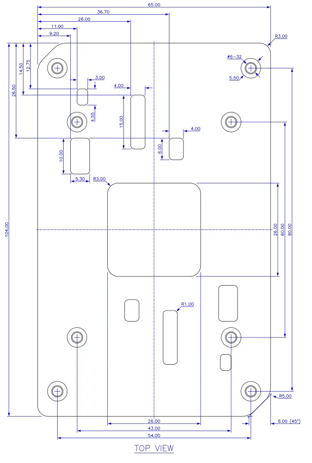
The stiffener frame has a window fitting the socket housing and incorporates a latch securing the lever in the actuated position. Four captive screws with #6-32 thread and Torx drive mount the stiffener frame to self-clinching PEM nuts protruding up from the backplate through holes in the PCB. Backplates with different nut heights are available to account for different PCB thicknesses. Two 0.18 mm thick insulating sheets in the shape of these parts separate them from the PCB.
Like Socket SP3 and SP5 the SAM apparently includes an external cap protecting the contact springs when no processor is installed.
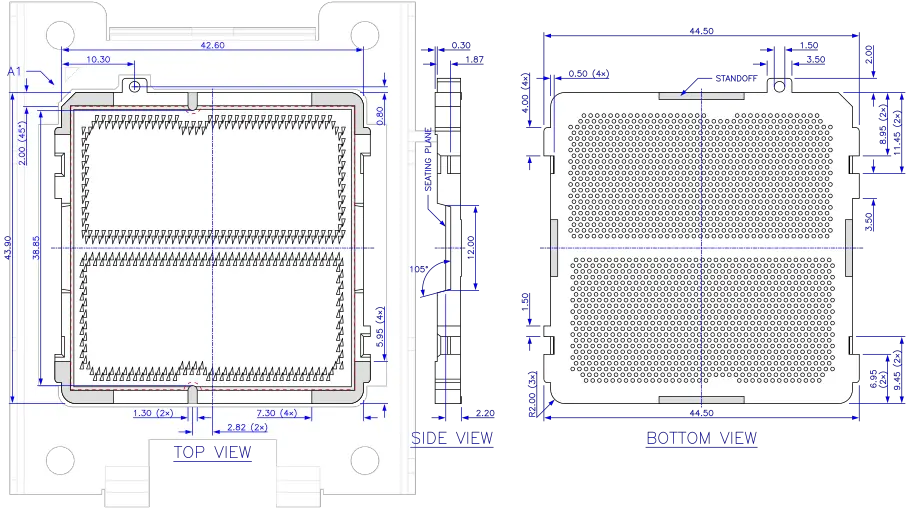
The socket housing is an injection-molded plastic part, likely made of black liquid crystal polymer, and ships with a cover cap made of the same material which protects the contact springs and facilitates pick-and-place operation with a vacuum nozzle during board assembly. The housing outline is asymmetric, preventing the SAM and cover cap from being installed rotated. The walls have finger access cut-outs, keying features matching those on the CPU package, and a chamfered corner locating pin A1. Four undercut steps on the outside and an alignment hole suggest corresponding latches and an alignment peg on the cover cap. The springs extend into a J-lead at the bottom of the housing with solder balls attached for surface mounting. Standoffs limit the distance to the PCB.
Heatsink
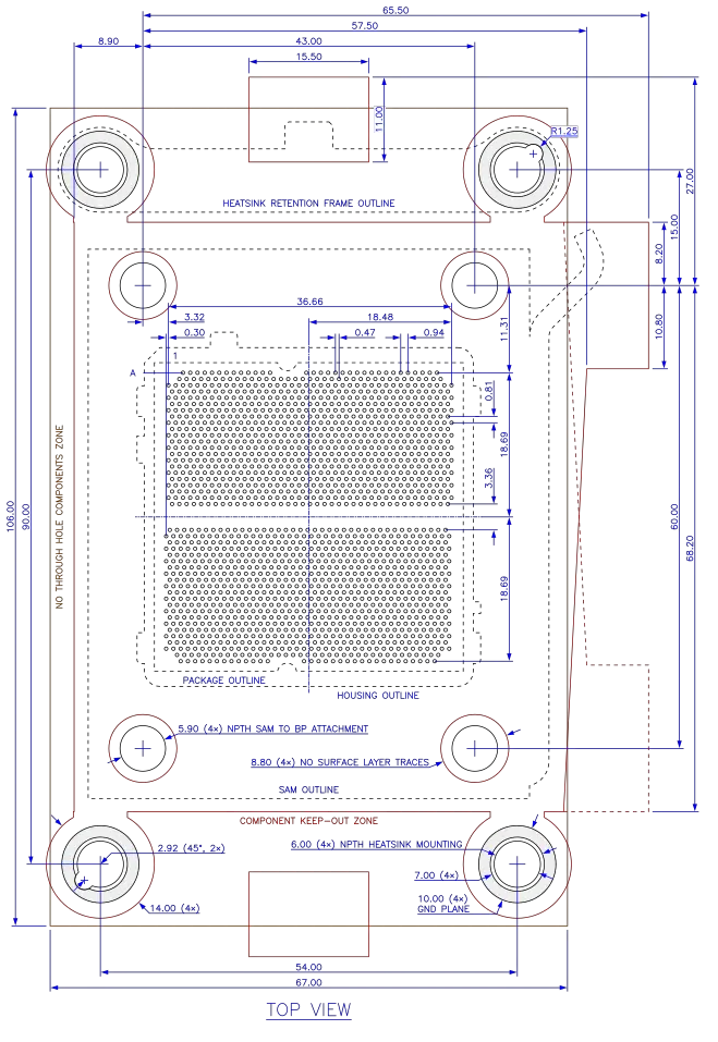
The heatsink can be clipped onto a two-part retention frame made of plastic. The two-part design permits components closer to the socket and smaller boards. Each of the identical parts has an alignment peg preventing it from being installed rotated on the PCB which has correspondingly shaped through-holes. Two screws with #6-32 thread (like PC case screws; the closest metric substitute is the non-standard M3.5×0.8 thread) mount each part to a second set of taller PEM nuts, spaced 54 mm × 90 mm apart, which protrude up through the PCB from the backplate. Their height is some 5 mm leaving 4.34 mm headroom to the top of the package lid in the actuated socket. Heavier heatsinks can be attached directly to the backplate with four captive spring screws on the heatsink after removal of the retention frame. The positions of the retention frame latches and heatsink nuts are symmetric so the heatsink can be rotated 180 degrees.
The heatsink attachment facilities and the height of the processor in the actuated socket, 7.98 ± 0.60 mm from the top of the PCB to the top of the lid, are in line with Socket AM4 so heatsinks for that socket can be used.
Feature Summary
- Lidded land grid array package, 40 mm × 40 mm
- 1718 contacts in a 44 × 40 grid, 0.81 mm × 0.94 mm interstitial pitch
- Organic substrate, flip chip die attachment
- 2 × 64/72 bit DDR5 SDRAM interface
- Data rate up to ?
- Two DDR5 subchannels per DRAM channel, 32 bit data + 4 bit ECC
- Up to 2 DIMMs/channel, up to 4 DIMMs total
- SR/DR UDIMM or SO-DIMM types
- Max. total memory capacity ? GiB using four ? GiB DIMMs
- PCIe Gen 4/5 (32 GT/s)
- 16 lane graphics card interface, configurable 1x16, 2x8
- 2 × 4 lanes general purpose (e.g. for M.2 NVME, PCIe slot, USB4 PCIe tunneling)
- 4 lane chipset interface
- Up to four digital display interfaces
- Five USB ports from three or four USB controllers
- 2 × USB 2.0, 3.2 Gen 1/2, USB4 (40 Gb/s), Type-C support, DP Alt Mode
- 1 × USB 2.0, 3.2 Gen 1/2 (10 Gb/s), Type-C, DP Alt Mode
- 1 × USB 2.0, 3.2 Gen 1/2 (10 Gb/s), Type-A
- 1 × USB 2.0
- Low speed interfaces (some sharing pins):
Note some processor models support only a subset of these features.
Chipsets
| This section is empty; you can help add the missing info by editing this page. |
Processors using Socket AM5
| Model | Family | Microarch. | Cores | Threads | L2$ | L3$ | Base | Turbo | Memory | TDP | Launched | Price | OPN |
|---|---|---|---|---|---|---|---|---|---|---|---|---|---|
| 7700 | Ryzen 7 | Zen 4 | 8 | 16 | 8 MiB 8,192 KiB 8,388,608 B 0.00781 GiB | 32 MiB 32,768 KiB 33,554,432 B 0.0313 GiB | 3.8 GHz 3,800 MHz 3,800,000 kHz | 5.3 GHz 5,300 MHz 5,300,000 kHz | 65 W 65,000 mW 0.0872 hp 0.065 kW | 10 January 2023 | $ 339.00 € 305.10 £ 274.59 ¥ 35,028.87 | 100-000000592, 100-100000592BOX | |
| 7700X | Ryzen 7 | Zen 4 | 8 | 16 | 8 MiB 8,192 KiB 8,388,608 B 0.00781 GiB | 32 MiB 32,768 KiB 33,554,432 B 0.0313 GiB | 4.5 GHz 4,500 MHz 4,500,000 kHz | 5.4 GHz 5,400 MHz 5,400,000 kHz | 105 W 105,000 mW 0.141 hp 0.105 kW | 27 September 2022 | $ 399.00 € 359.10 £ 323.19 ¥ 41,228.67 | 100-000000591, 100-100000591WOF | |
| 7950X3D | Ryzen 9 | Zen 4 | 16 | 32 | 16 MiB 16,384 KiB 16,777,216 B 0.0156 GiB | 128 MiB 131,072 KiB 134,217,728 B 0.125 GiB | 4.2 GHz 4,200 MHz 4,200,000 kHz | 5.7 GHz 5,700 MHz 5,700,000 kHz | 120 W 120,000 mW 0.161 hp 0.12 kW | 28 February 2023 | $ 699.00 € 629.10 £ 566.19 ¥ 72,227.67 | 100-000000908, 100-000000908WOF | |
| Count: 3 |
Photos
| This section is empty; you can help add the missing info by editing this page. |
Package Diagrams
AM5 package. All dimensions in millimeters.
Socket Diagrams
Socket AM5 housing (AMD). All dimensions in millimeters.
Socket AM5 backplate. All dimensions in millimeters.
Socket AM5 PCB layout. NPTH = Non-Plated Through Hole. All dimensions in millimeters.
Pin Map
| This section is empty; you can help add the missing info by editing this page. |
Pin Description
| Signal | Description | ||||
|---|---|---|---|---|---|
| MA/MB_ALERT_L | DRAM Channel A/B Alert (CRC error and Command/Address parity error) | ||||
| MA/MB_RESET_L | DRAM Channel A/B DIMM Reset | ||||
| MAA/MAB/MBA/MBB_CA[13:0] | DRAM Channel A/B Subchannel A/B Command/Address Bus | ||||
| MAA/MAB/MBA/MBB_CHECK[3:0] | DRAM Channel A/B Subchannel A/B ECC Check Byte | ||||
| MAA/MAB/MBA/MBB_DATA[31:0] | DRAM Channel A/B Subchannel A/B Data Bus | ||||
| MAA/MAB/MBA/MBB_DM[3:0] | DRAM Channel A/B Subchannel A/B Data Mask | ||||
| MAA/MAB/MBA/MBB_DQS_H/L[4:0] | DRAM Channel A/B Subchannel A/B Data Strobe Differential Pair | ||||
| MAA0/MAB0/MBA0/MBB0_CLK_H/L[1:0] MAA1/MAB1/MBA1/MBB1_CLK_H/L[1:0] |
DRAM Channel A/B DIMM 0/1 Subchannel A/B Differential Clock | ||||
| MAA0/MAB0/MBA0/MBB0_CS_L[1:0] MAA1/MAB1/MBA1/MBB1_CS_L[1:0] |
DRAM Channel A/B DIMM 0/1 Subchannel A/B Chip Select | ||||
| PCIE_RXP/RXN[27:0] | PCIe Receive Data Differential Pairs | ||||
| PCIE_TXP/TXN[27:0] | PCIe Transmit Data Differential Pairs | ||||
| PCIE_RST0_L | Reset for PCIe devices or SPI TPM | ||||
| DP0-DP3_TXP/TXN[3:0] | DisplayPort 0-3 Main Link Differential Transmitter Lane 0-3 or DVI/HDMI Channel 2, 1, 0, Clock | ||||
| DP0-DP3_AUXP/AUXN | DisplayPort 0-3 Auxiliary Channel or DVI/HDMI DDC Clock, Data | ||||
| DP0-DP3_HPD | DisplayPort 0-3 Hot Plug Detect Input | ||||
| DP0_BLON | Display Panel Backlight Enable | ||||
| DP0_DIGON | Display Panel Power Enable | ||||
| DP0_VARY_BL | Display Backlight Brightness Control | ||||
| DP_STEREOSYNC | StereoSync output for shutter glasses | ||||
| USBC(0-2)_RX1P/RX1N | USB Port 0-2 USB-C Receive Differential Pairs or DisplayPort Transmitter Lane 3 | ||||
| USBC(0-2)_TX1P/TX1N | USB Port 0-2 USB-C Transmit Differential Pairs or DisplayPort Transmitter Lane 2 | ||||
| USBC(0-2)_RX2P/RX2N | USB Port 0-2 USB-C Receive Differential Pairs or DisplayPort Transmitter Lane 0 | ||||
| USBC(0-2)_TX2P/TX2N | USB Port 0-2 USB-C Transmit Differential Pairs or DisplayPort Transmitter Lane 1 | ||||
| USB3_RXP/RXN | USB Port 3 USB3 Super Speed Receive Differential Pairs | ||||
| USB3_TXP/TXN | USB Port 3 USB3 Super Speed Transmit Differential Pairs | ||||
| USB(0-4)_DP/DN | USB Port 0-4 USB2 I/O Differential Pairs | ||||
| USBC0/USBC1_SBRX/SBTX | USB Port 0-1 USB4 Sideband Interface Differential Pairs (alt. func. of DP1_AUX, DP2_AUX) | ||||
| USBC_I2C_SCL | I2C Clock for USB-C PD Control | ||||
| USBC_I2C_SDA | I2C Data for USB-C PD Control | ||||
| USBC_PD_INT | USB-C Power Delivery Interrupt | ||||
| USB_BIOS_UPDATE | USB BIOS Update Function (momentary switch) | ||||
| USB_OC(0-3)_L | USB Over Current signal from USB connector | ||||
| AZ_BITCLK | Azalia HD Audio Interface Bit Clock | ||||
| AZ_RST_L | HDA Reset | ||||
| AZ_SDIN(0-2) | HDA Serial Data Input from Codec 0-2 | ||||
| AZ_SDOUT | HDA Serial Data Output to Codec | ||||
| AZ_SYNC | HDA Sync signal to Codec | ||||
| DMIC_CLK | Digital Microphone Clock Output | ||||
| DMIC_DATA0 | DMIC Data Input (2 ch PDM) | ||||
| DMIC_DATA1 | DMIC Data (alt. func. of AZ_BITCLK or AZ_SDIN1) | ||||
| DMIC_DATA2 | DMIC Data (AZ_SYNC or AZ_SDIN2) | ||||
| SW0_MCLK | SoundWire Interface 0 Clock (AZ_SDIN1) | ||||
| SW0_MDATA(0-3) | SW0 Data (AZ_SDIN2, AZ_RST_L, AZ_SDOUT, AZ_SDIN0) | ||||
| SW1_MCLK | SoundWire Interface 1 Clock (AZ_BITCLK) | ||||
| SW1_MDATA0 | SW1 Data (AZ_SYNC) | ||||
| SPKR | PC speaker/beeper PWM output | ||||
| SPI/SPI1_CLK | SPI Clock Output | ||||
| SPI/SPI1_DAT[0] | SPI Data 0 for multi-I/O device or Data Out | ||||
| SPI/SPI1_DAT[1] | SPI Data 1 for multi-I/O device or Data In | ||||
| SPI/SPI1_DAT[3:2] | SPI Data 2, 3 for multi-I/O device | ||||
| SPI/SPI1_CS(1-2)_L | Chip Select for SPI ROM | ||||
| SPI_TPM_CS_L | Chip Select for SPI TPM | ||||
| SPI_ROM_REQ | SPI ROM Request | ||||
| SPI_ROM_GNT | SPI ROM Grant | ||||
| ESPI_CLK | Enhanced SPI Clock Output | ||||
| ESPI_DAT[3:0] | ESPI Data[0], Data[1:0], Data[3:0] Input/Output | ||||
| ESPI_CS_L | ESPI Chip Select | ||||
| ESPI_ALERT_L | ESPI Alert Input | ||||
| ESPI_RESET_L | ESPI Reset Input (ESPI_RESET_L/KBRST_L) | ||||
| I3C(0-3)_SCL | I3C Bus 0-3 Clock | ||||
| I3C(0-3)_SDA | I3C Bus 0-3 Data | ||||
| I2C(0-3)_SCL | I2C Bus 0-3 Clock (alt. func. of I3C0-I3C3) | ||||
| I2C(0-3)_SDA | I2C Bus 0-3 Data | ||||
| SMBUS(0-1)_SCL | SMBus 0-1 Clock (I3C2, I3C3) | ||||
| SMBUS(0-1)_SDA | SMBus Data | ||||
| AGPIO* | Advanced GPIO pin for interrupt, wake, or I/O | ||||
| EGPIO* | Enhanced GPIO for I/O only | ||||
| GPP_CLK(0-5)P/N | 100 MHz Differential PCIe Reference Clock Outputs | ||||
| CLK_REQ(0-5)_L | PCIe Clock Request | ||||
| X32K_X1/X2 | 32768 Hz Real Time Clock XTAL | ||||
| X48M_X1/X2 | 48 MHz clock XTAL for the integrated clock generator | ||||
| X48M_OSC | 48 MHz clock output for devices requiring a single-ended OSC input | ||||
| RTCCLK | 32768 Hz Real Time Clock output for a device requiring an RTC clock | ||||
| BLINK | Blink LED S-state Indicator | ||||
| KBRST_L | Keyboard Controller Reset Input (warm reset) | ||||
| PWR_GOOD | Power Good Input; Asserted when all voltages are within specification | ||||
| PWR_BTN_L | Power Button Input; Requests sleep state or causes wake event | ||||
| RESET_L | Reset signal | ||||
| RSMRST_L | Resume Reset; Asserted on power up, deasserted when S5 power supplies are within specification | ||||
| S0A3_GPIO | |||||
| SLP_S3/S5_L | S3/S5 Sleep State Power Plane Control Signals for voltage regulator | ||||
| SYS_RESET_L | System Reset Input (reset button) | ||||
| WAKE(0-3)_L | PCIe WAKE_L signal, wake system out of sleep state | ||||
| WAKE(4-5)_L | PCIe WAKE_L signal (alt. func. of USB_OC1, USB_OC2) | ||||
| ALERT_L | SB-TSI Interrupt | ||||
| FANIN0 | Fan 0 tachometer input | ||||
| FANOUT0 | Fan 0 PWM output | ||||
| PROCHOT_L | Asserted to force the processor into HTC-active state | ||||
| SIC | Sideband Interface (SB-TSI) Clock | ||||
| SID | Sideband Interface Data | ||||
| THERMTRIP_L | Temperature Trip Output | ||||
| TCK | JTAG Clock | ||||
| TDI | JTAG Data Input | ||||
| TDO | JTAG Data Output | ||||
| TMS | JTAG Mode Select | ||||
| TRST_L | JTAG Reset | ||||
| TEST* | Test/Debug signals | ||||
| SVC | Serial VID Clock for VDDCR/VDDCR_SOC regulator | ||||
| SVD | Serial VID Data | ||||
| SVT | Serial VID Telemetry | ||||
| VDDBT_RTC_G | Integrated Real Time Clock battery power supply | ||||
| VDDCR | Core power supply | ||||
| VDDCR_SENSE | Differential (with VSS_SENSE_A) feedback for VDDCR regulator | ||||
| VDDCR_SOC | Power supply for integrated Northbridge | ||||
| VDDCR_SOC_SENSE | Differential (with VSS_SENSE_A) feedback for VDDCR_SOC regulator | ||||
| VDDIO_AUDIO | |||||
| VDDIO_MEM_S3 | |||||
| VDDIO_MEM_S3_SENSE | |||||
| VDD_18 | 1.8 V supply voltage for analog circuits | ||||
| VDD_18_S5 | Always on 1.8 V supply voltage for analog circuits | ||||
| VDD_33 | 3.3 V supply voltage | ||||
| VDD_33_S5 | Always on 3.3 V supply voltage | ||||
| VDD_MISC | Power supply for DisplayPort and PCIe PHY logic | ||||
| VDD_MISC_SENSE | Differential feedback for VDD_MISC regulator | ||||
| VDD_MISC_S5 | Power supply for USB physical layer | ||||
| VDD_MISC_S5_SENSE | Differential (with VSS_SENSE_B) feedback for VDD_MISC_S5 regulator | ||||
| VSS_SENSE_A | VSS Sense pin for VDDCR/VDDCR_SOC regulator | ||||
| VSS_SENSE_B | VSS Sense pin for VDD_MISC regulator | ||||
| AM5R1 | Processor family revision identifier; NC = Not connected, VSS = connected to VSS on the package
| ||||
| RSVD | Reserved |
Bibliography
See also
| designer | AMD + |
| first launched | April 18, 2022 + |
| instance of | package + |
| market segment | Desktop + |
| microarchitecture | Zen 4 + |
| name | Socket AM5 + |
| package | LGA-1718 + |
| package contacts | 1,718 + |
| package length | 40 mm (4 cm, 1.575 in) + |
| package pitch | 0.81 mm (0.0319 in) + and 0.94 mm (0.037 in) + |
| package type | FC-OLGA + |
| package width | 40 mm (4 cm, 1.575 in) + |
| socket | Socket AM5 + |
| tdp | 170 W (170,000 mW, 0.228 hp, 0.17 kW) + |


