From WikiChip
Difference between revisions of "intel/xeon platinum/8270"
| Line 8: | Line 8: | ||
|part number=CD8069504195201 | |part number=CD8069504195201 | ||
|s-spec=SRF96 | |s-spec=SRF96 | ||
| + | |s-spec qs=QRAU | ||
|market=Server | |market=Server | ||
|first announced=April 2, 2019 | |first announced=April 2, 2019 | ||
| Line 26: | Line 27: | ||
|core name=Cascade Lake SP | |core name=Cascade Lake SP | ||
|core family=6 | |core family=6 | ||
| − | |core stepping=B1 | + | |core stepping=B0 |
| + | |core stepping 2=B1 | ||
|process=14 nm | |process=14 nm | ||
|technology=CMOS | |technology=CMOS | ||
| Line 32: | Line 34: | ||
|core count=26 | |core count=26 | ||
|thread count=52 | |thread count=52 | ||
| + | |max memory=1 TiB | ||
|max cpus=8 | |max cpus=8 | ||
| − | | | + | |smp interconnect=UPI |
| + | |smp interconnect links=3 | ||
| + | |smp interconnect rate=10.4 GT/s | ||
|tdp=205 W | |tdp=205 W | ||
|package name 1=intel,fclga_3647 | |package name 1=intel,fclga_3647 | ||
Latest revision as of 01:53, 29 December 2019
| Edit Values | |
| Xeon Platinum 8270 | |
 | |
| General Info | |
| Designer | Intel |
| Manufacturer | Intel |
| Model Number | 8270 |
| Part Number | CD8069504195201 |
| S-Spec | SRF96 QRAU (QS) |
| Market | Server |
| Introduction | April 2, 2019 (announced) April 2, 2019 (launched) |
| Release Price | $7,405.00 (tray) |
| Shop | Amazon |
| General Specs | |
| Family | Xeon Platinum |
| Series | 8200 |
| Locked | Yes |
| Frequency | 2,700 MHz |
| Turbo Frequency | 4,000 MHz (1 core) |
| Clock multiplier | 27 |
| CPUID | 0x50655 |
| Microarchitecture | |
| ISA | x86-64 (x86) |
| Microarchitecture | Cascade Lake |
| Platform | Purley |
| Chipset | Lewisburg |
| Core Name | Cascade Lake SP |
| Core Family | 6 |
| Core Stepping | B0, B1 |
| Process | 14 nm |
| Technology | CMOS |
| Word Size | 64 bit |
| Cores | 26 |
| Threads | 52 |
| Max Memory | 1 TiB |
| Multiprocessing | |
| Max SMP | 8-Way (Multiprocessor) |
| Interconnect | UPI |
| Interconnect Links | 3 |
| Interconnect Rate | 10.4 GT/s |
| Electrical | |
| TDP | 205 W |
| Packaging | |
| Package | FCLGA-3647 (FCLGA) |
| Dimension | 76.16 mm × 56.6 mm |
| Pitch | 0.8585 mm × 0.9906 mm |
| Contacts | 3647 |
| Socket | Socket P, LGA-3647 |
| Succession | |
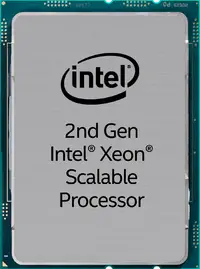
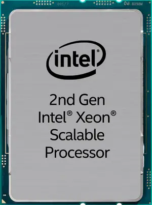
Xeon Platinum 8270 is a 64-bit 26-core x86 high-performance server microprocessor introduced by Intel in early 2019. The Platinum 8270 is based on the Cascade Lake microarchitecture and is manufactured on a 14 nm process. This chip supports 8-way multiprocessing, sports 2 AVX-512 FMA units as well as three Ultra Path Interconnect links. This microprocessor supports up 1 TiB of hexa-channel DDR4-2933 memory, operates at 2.7 GHz with a TDP of 205 W and features a turbo boost frequency of up to 4.0 GHz.
Cache[edit]
- Main article: Cascade Lake § Cache
|
Cache Organization
Cache is a hardware component containing a relatively small and extremely fast memory designed to speed up the performance of a CPU by preparing ahead of time the data it needs to read from a relatively slower medium such as main memory. The organization and amount of cache can have a large impact on the performance, power consumption, die size, and consequently cost of the IC. Cache is specified by its size, number of sets, associativity, block size, sub-block size, and fetch and write-back policies. Note: All units are in kibibytes and mebibytes. |
|||||||||||||||||||||||||||||||||||||
|
|||||||||||||||||||||||||||||||||||||
Memory controller[edit]
|
Integrated Memory Controller
|
||||||||||||||
|
||||||||||||||
Expansions[edit]
Expansion Options |
|||||
|
|||||
Features[edit]
[Edit/Modify Supported Features]
Frequencies[edit]
- See also: Intel's CPU Frequency Behavior
| Mode | Base | Turbo Frequency/Active Cores | |||||||||||||||||||||||||
|---|---|---|---|---|---|---|---|---|---|---|---|---|---|---|---|---|---|---|---|---|---|---|---|---|---|---|---|
| 1 | 2 | 3 | 4 | 5 | 6 | 7 | 8 | 9 | 10 | 11 | 12 | 13 | 14 | 15 | 16 | 17 | 18 | 19 | 20 | 21 | 22 | 23 | 24 | 25 | 26 | ||
| Normal | 2,700MHz | 4,000MHz | 4,000MHz | 3,800MHz | 3,800MHz | 3,700MHz | 3,700MHz | 3,700MHz | 3,700MHz | 3,700MHz | 3,700MHz | 3,700MHz | 3,700MHz | 3,700MHz | 3,700MHz | 3,700MHz | 3,700MHz | 3,700MHz | 3,700MHz | 3,700MHz | 3,700MHz | 3,500MHz | 3,500MHz | 3,500MHz | 3,500MHz | 3,400MHz | 3,400MHz |
| AVX2 | 2,200MHz | 3,800MHz | 3,800MHz | 3,600MHz | 3,600MHz | 3,500MHz | 3,500MHz | 3,500MHz | 3,500MHz | 3,500MHz | 3,500MHz | 3,500MHz | 3,500MHz | 3,400MHz | 3,400MHz | 3,400MHz | 3,400MHz | 3,200MHz | 3,200MHz | 3,200MHz | 3,200MHz | 2,900MHz | 2,900MHz | 2,900MHz | 2,900MHz | 2,900MHz | 2,900MHz |
| AVX512 | 1,800MHz | 3,700MHz | 3,700MHz | 3,500MHz | 3,500MHz | 3,400MHz | 3,400MHz | 3,400MHz | 3,400MHz | 3,200MHz | 3,200MHz | 3,200MHz | 3,200MHz | 2,800MHz | 2,800MHz | 2,800MHz | 2,800MHz | 2,600MHz | 2,600MHz | 2,600MHz | 2,600MHz | 2,400MHz | 2,400MHz | 2,400MHz | 2,400MHz | 2,400MHz | 2,400MHz |
Facts about "Xeon Platinum 8270 - Intel"
| Has subobject "Has subobject" is a predefined property representing a container construct and is provided by Semantic MediaWiki. | Xeon Platinum 8270 - Intel#pcie + |
| base frequency | 2,700 MHz (2.7 GHz, 2,700,000 kHz) + |
| chipset | Lewisburg + |
| clock multiplier | 27 + |
| core count | 26 + |
| core family | 6 + |
| core name | Cascade Lake SP + |
| core stepping | B0 + and B1 + |
| cpuid | 0x50655 + |
| designer | Intel + |
| family | Xeon Platinum + |
| first announced | April 2, 2019 + |
| first launched | April 2, 2019 + |
| full page name | intel/xeon platinum/8270 + |
| has advanced vector extensions | true + |
| has advanced vector extensions 2 | true + |
| has advanced vector extensions 512 | true + |
| has ecc memory support | true + |
| has extended page tables support | true + |
| has feature | Advanced Vector Extensions +, Advanced Vector Extensions 2 +, Advanced Vector Extensions 512 +, Advanced Encryption Standard Instruction Set Extension +, Hyper-Threading Technology +, Turbo Boost Technology 2.0 +, Enhanced SpeedStep Technology +, Speed Shift Technology +, Trusted Execution Technology +, Intel vPro Technology +, Intel VT-x +, Intel VT-d +, Extended Page Tables +, Transactional Synchronization Extensions + and Deep Learning Boost + |
| has intel deep learning boost | true + |
| has intel enhanced speedstep technology | true + |
| has intel speed shift technology | true + |
| has intel trusted execution technology | true + |
| has intel turbo boost technology 2 0 | true + |
| has intel vpro technology | true + |
| has intel vt-d technology | true + |
| has intel vt-x technology | true + |
| has locked clock multiplier | true + |
| has second level address translation support | true + |
| has simultaneous multithreading | true + |
| has transactional synchronization extensions | true + |
| has x86 advanced encryption standard instruction set extension | true + |
| instance of | microprocessor + |
| isa | x86-64 + |
| isa family | x86 + |
| l1$ size | 1,664 KiB (1,703,936 B, 1.625 MiB) + |
| l1d$ description | 8-way set associative + |
| l1d$ size | 832 KiB (851,968 B, 0.813 MiB) + |
| l1i$ description | 8-way set associative + |
| l1i$ size | 832 KiB (851,968 B, 0.813 MiB) + |
| l2$ description | 16-way set associative + |
| l2$ size | 26 MiB (26,624 KiB, 27,262,976 B, 0.0254 GiB) + |
| l3$ description | 11-way set associative + |
| l3$ size | 35.75 MiB (36,608 KiB, 37,486,592 B, 0.0349 GiB) + |
| ldate | April 2, 2019 + |
| main image |  + + |
| manufacturer | Intel + |
| market segment | Server + |
| max cpu count | 8 + |
| max memory | 1,048,576 MiB (1,073,741,824 KiB, 1,099,511,627,776 B, 1,024 GiB, 1 TiB) + |
| max memory bandwidth | 131.13 GiB/s (134,277.12 MiB/s, 140.8 GB/s, 140,799.765 MB/s, 0.128 TiB/s, 0.141 TB/s) + |
| max memory channels | 6 + |
| microarchitecture | Cascade Lake + |
| model number | 8270 + |
| name | Xeon Platinum 8270 + |
| number of avx-512 execution units | 2 + |
| package | FCLGA-3647 + |
| part number | CD8069504195201 + |
| platform | Purley + |
| process | 14 nm (0.014 μm, 1.4e-5 mm) + |
| release price | $ 7,405.00 (€ 6,664.50, £ 5,998.05, ¥ 765,158.65) + |
| release price (tray) | $ 7,405.00 (€ 6,664.50, £ 5,998.05, ¥ 765,158.65) + |
| s-spec | SRF96 + |
| s-spec (qs) | QRAU + |
| series | 8200 + |
| smp interconnect | UPI + |
| smp interconnect links | 3 + |
| smp interconnect rate | 10.4 GT/s + |
| smp max ways | 8 + |
| socket | Socket P + and LGA-3647 + |
| supported memory type | DDR4-2933 + |
| tdp | 205 W (205,000 mW, 0.275 hp, 0.205 kW) + |
| technology | CMOS + |
| thread count | 52 + |
| turbo frequency (1 core) | 4,000 MHz (4 GHz, 4,000,000 kHz) + |
| word size | 64 bit (8 octets, 16 nibbles) + |