(→NPU) |
|||
| Line 26: | Line 26: | ||
|package name 1=tesla_car,fcbga_2116 | |package name 1=tesla_car,fcbga_2116 | ||
}} | }} | ||
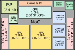
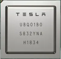
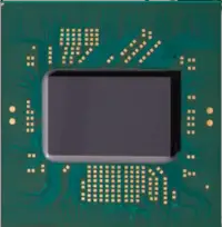
| − | '''Full Self-Driving Chip''' ('''FSD Chip''', previously '''Autopilot Hardware 3.0''') is an [[autonomous machine chip]] designed by [[tesla car|Tesla]] and announced and introduced in early [[2019]] for their cars. Fabricated on [[Samsung]]'s [[14 nm process technology]], | + | '''Full Self-Driving Chip''' ('''FSD Chip''', previously '''Autopilot Hardware 3.0''') is an [[autonomous machine chip]] designed by [[tesla car|Tesla]] and announced and introduced in early [[2019]] for their cars. Fabricated on [[Samsung]]'s [[14 nm process technology]], the FSD Chip incorporates 3 quad-core {{armh|Cortex-A72|l=arch}} clusters for a total of 12 CPUs operating at 2.2 GHz, a GPU operating 1 GHz, 2 [[neural processing units]] operating at 2 GHz, and various other hardware accelerators. The FSD supports up to octa-channel LPDDR4-4266 memory. |
== History == | == History == | ||
| Line 35: | Line 35: | ||
The full self-driving chip or FSD chip for short is [[tesla car|Tesla's]] home-grown custom designed [[autonomous driving chip]]. The chip has been in development since [[2016]] and has entered mass production in early [[2019]]. Designed as a drop-in upgrade for Tesla's existing cars, the FSD chip inherits most of the power and thermal requirements of prior solutions - including staying with the maximum power consumption of 100 W. Since the chip itself is designed specifically for Tesla's own cars and their own requirements, much of the general purpose-ability of alternative [[neural processors]] has been stripped away from the FSD chip, leaving the design with only the hardware they need. | The full self-driving chip or FSD chip for short is [[tesla car|Tesla's]] home-grown custom designed [[autonomous driving chip]]. The chip has been in development since [[2016]] and has entered mass production in early [[2019]]. Designed as a drop-in upgrade for Tesla's existing cars, the FSD chip inherits most of the power and thermal requirements of prior solutions - including staying with the maximum power consumption of 100 W. Since the chip itself is designed specifically for Tesla's own cars and their own requirements, much of the general purpose-ability of alternative [[neural processors]] has been stripped away from the FSD chip, leaving the design with only the hardware they need. | ||
| − | At a high level, the chip is a full system-on-a-chip capable of booting a standard operating system. It is manufactured on Samsung's [[14-nanometer process]] at their Austin, Texas fab, packing roughly six billion transistors on a 260 millimeter squared silicon die. The choice to go with a mature [[14 nm]] node instead of a more [[technology node|leading-edge node]] boiled down to cost and IP readiness. There are twelve {{arch|64}} [[ARM]] cores organized as three clusters of quad-core {{armh|Cortex-A72|l=arch}} cores operating at 2.2 GHz which are used for general purpose processing. There is also relatively light GPU primarily designed for light-weight post-processing. It operates at 1 GHz, capable of up to 600 GFLOPS, supporting both [[single-precision]] and [[double-precision]] floating point operations. | + | At a high level, the chip is a full system-on-a-chip capable of booting a standard operating system. It is manufactured on Samsung's [[14-nanometer process]] at their Austin, Texas fab, packing roughly six billion transistors on a 260 millimeter squared silicon die. The FSD chip meets AEC-Q100 automotive quality standards. The choice to go with a mature [[14 nm]] node instead of a more [[technology node|leading-edge node]] boiled down to cost and IP readiness. There are twelve {{arch|64}} [[ARM]] cores organized as three clusters of quad-core {{armh|Cortex-A72|l=arch}} cores operating at 2.2 GHz which are used for general purpose processing. There is also relatively light GPU primarily designed for light-weight post-processing. It operates at 1 GHz, capable of up to 600 GFLOPS, supporting both [[single-precision]] and [[double-precision]] floating point operations. |
The chip features a relatively low-cost conventional memory subsystem supporting 128-bit of LPDDR4 memory operating at 2133 MHz. | The chip features a relatively low-cost conventional memory subsystem supporting 128-bit of LPDDR4 memory operating at 2133 MHz. | ||
Revision as of 10:49, 27 April 2019
| Edit Values | |
| FSD Chip | |
 | |
 | |
| General Info | |
| Designer | Tesla (car company) |
| Manufacturer | Samsung |
| Market | Automotive |
| Introduction | April 22, 2019 (announced) March 10, 2019 (launched) |
| General Specs | |
| Frequency | 2,200 MHz |
| Microarchitecture | |
| ISA | ARMv8.0-A (ARM) |
| Microarchitecture | Cortex-A72 |
| Core Name | Cortex-A72 |
| Core Stepping | B0 |
| Process | 14 nm |
| Transistors | 6,000,000,000 |
| Technology | CMOS |
| Die | 260 mm² 20 mm × 13 mm |
| Word Size | 64 bit |
| Cores | 12 |
| Threads | 12 |
| Packaging | |
| Package | FCBGA-2116 (BGA) |
| Dimension | 37.5 mm × 37.5 mm |
| Contacts | 2116 |
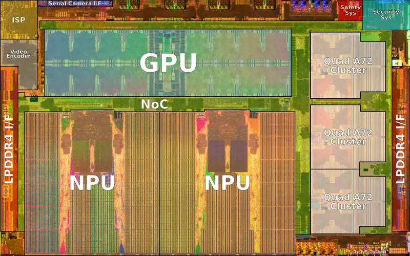
Full Self-Driving Chip (FSD Chip, previously Autopilot Hardware 3.0) is an autonomous machine chip designed by Tesla and announced and introduced in early 2019 for their cars. Fabricated on Samsung's 14 nm process technology, the FSD Chip incorporates 3 quad-core Cortex-A72 clusters for a total of 12 CPUs operating at 2.2 GHz, a GPU operating 1 GHz, 2 neural processing units operating at 2 GHz, and various other hardware accelerators. The FSD supports up to octa-channel LPDDR4-4266 memory.
Contents
History
Design and planning for the FSD chip started in 2016 when Tesla claims they saw no alternative solution that fits their problem of addressing autonomous driving. The FSD chip project was led by Pete Bannon. The design team was formed in February 2016. Development was done over the course of 18 months. In August 2017, the chip was released for manufacturing with first silicon coming back in December 2017 fully working. A number of additional modifications were done to the design, requiring respinning. B0 stepping was released to manufacturing in April 2018. Full production of B0 started shortly after qualifications in July 2018. In December 2018, Tesla started retrofitting employee cars with the new hardware and software stack. In March 2019, Tesla began volume shipping the FSD chip and computer in their Model S and Model X cars. Production shipment in the Tesla Model 3 started in April 2019.
Overview
The full self-driving chip or FSD chip for short is Tesla's home-grown custom designed autonomous driving chip. The chip has been in development since 2016 and has entered mass production in early 2019. Designed as a drop-in upgrade for Tesla's existing cars, the FSD chip inherits most of the power and thermal requirements of prior solutions - including staying with the maximum power consumption of 100 W. Since the chip itself is designed specifically for Tesla's own cars and their own requirements, much of the general purpose-ability of alternative neural processors has been stripped away from the FSD chip, leaving the design with only the hardware they need.
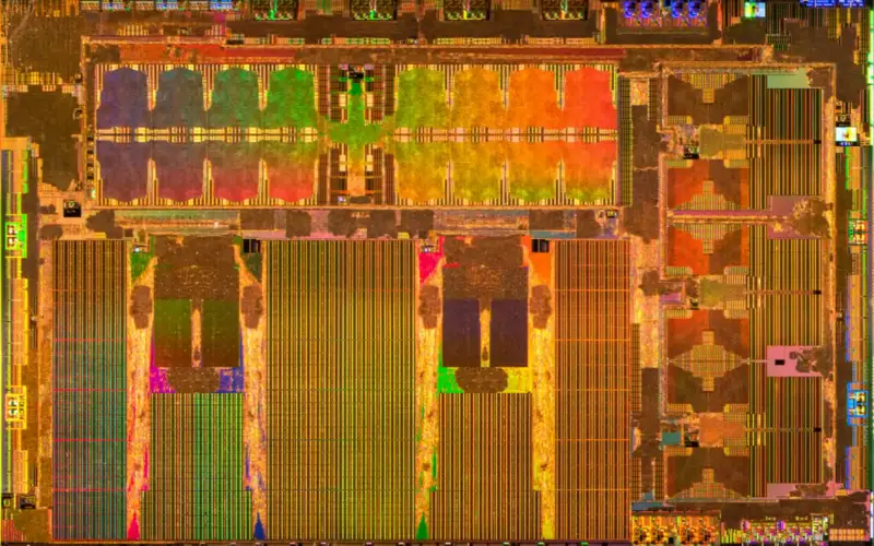
At a high level, the chip is a full system-on-a-chip capable of booting a standard operating system. It is manufactured on Samsung's 14-nanometer process at their Austin, Texas fab, packing roughly six billion transistors on a 260 millimeter squared silicon die. The FSD chip meets AEC-Q100 automotive quality standards. The choice to go with a mature 14 nm node instead of a more leading-edge node boiled down to cost and IP readiness. There are twelve 64-bit ARM cores organized as three clusters of quad-core Cortex-A72 cores operating at 2.2 GHz which are used for general purpose processing. There is also relatively light GPU primarily designed for light-weight post-processing. It operates at 1 GHz, capable of up to 600 GFLOPS, supporting both single-precision and double-precision floating point operations.
The chip features a relatively low-cost conventional memory subsystem supporting 128-bit of LPDDR4 memory operating at 2133 MHz.
Safety system
There is a safety system that incorporates a dual-core lockstep CPU which conducts the final arbitration of the car actuators. This CPU determines if the two plans generated by the two FSD chips on the FSD computer match and if it's safe to drive the actuators.
Security system
The security system is designed to ensure the chip only executes code that has been cryptographically-signed by Tesla
Camera serial interface
The FSD chip has a camera serial interface (CSI) capable of up to 2.5 billion pixels per second from the various video input devices for processing.
Video Encoder
The FSD chip integrates an H.265 (HEVC) video encoder which is used for various applications such as the back up camera display, dash cam, and cloud clip-logging.
Image signal processor
The FSD incorporates an image signal processor (ISP) with an internal 24-bit pipeline designed to process the eight HDR sensors equipped on Tesla cars and is capable of processing up to a billion pixels per second. The ISP has tone mapping capabilities, allowing the chip to expose additional details due to bright/dark spots such as shadows. Additionally, the ISP has noise reduction capabilities.
Neural processing unit
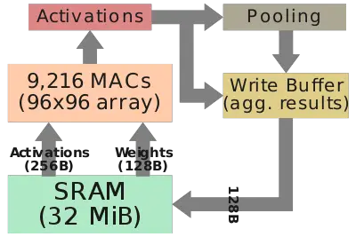
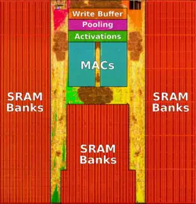
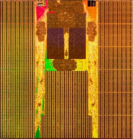
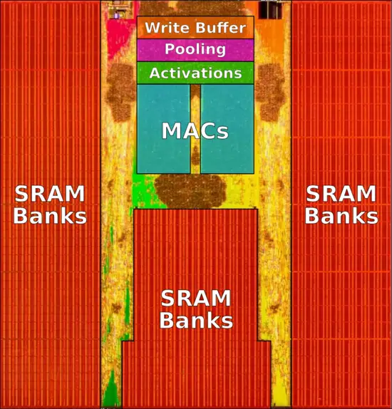
The FSD chip integrates two custom-designed neural processing units. Each NPU packs 32 MiB of SRAM designed for storing temporary network results, reducing data movements to main memory. The overall design is pretty straightforward. Each cycle, 256 bytes of activation data and an additional 128 bytes of weight data is read from the SRAM into the MACs array where they are combined. Each NPU has a 96x96 multiplay-accumulate array for a total of 9,216 MACs and 18,432 operations. For the FSD chip, Tesla uses an 8-bit by 8-bit integer multiply and a 32-bit integer addition. The choices for both data types is largely driven by their effort to reduce the power consumption (e.g., a 32-bit FP addition consumes roughly 9 times as much as a 32-bit integer addition) Operating at 2 GHz, each NPU has a peak performance of 36.86 trillion operations per second (TOPS). With two NPUs on each chip, the FSD chip is capable of up to 73.7 trillion operations per second of combined peak performance. Following the dot product operation, data is shifted to the activation hardware, the pooling hardware, and finally into the write buffer which aggregates the results. The FSD supports a number of activation functions, including a rectified linear unit (ReLU), Sigmoid Linear Unit (SiLU), and TanH. Each cycle, 128 bytes of result data is written back to the SRAM. All the operations are done simultaneously and continuously, repeating until the full network is done.
Some of the hardware has been simplified which puts the complexity onto the software. This was done to reduce the cost of silicon in favor of slightly more complex software. The software can map and allocate individual SRAM banks. With the help of Tesla's NN compiler, layer fusion is also done, allowing data reuse by coupling conv-scale-act-pooling operations. The compiler also performs layer smoothing, ensuring consistent memory accesses, adds channel padding designed to reduce bank conflicts, and inserts DMA operations to prefetch data prior to use. During code generation, weight data is generated, code is compressed, and a CRC checksum is generated for reliability.
Under normal operation, the neural network program is loaded at the start and is kept in memory for the entire duration in which the chip is powered. Running is done by setting the input buffers address (e.g., newly taken image sensor photo), setting the output buffer address, and weight buffer address (e.g., network weights), set the program address, and run. The NPU will asynchronously run on its own the entire neural network model until reaching a stop instruction which triggers an interrupt, letting the CPU post-process the results.
Instruction set
The NPU includes a small instruction set to efficiently process convolutional neural networks.
- 2 x DMA operations for reading and writing to main memory
- 3x dot-product instructions (convolution, deconvolution, and innner-product)
- scale (1-input, 1-output)
- eltwise (2-input, 1-output)
- stop to half processing.
Memory controller
|
Integrated Memory Controller
|
||||||||||||||
|
||||||||||||||
Full self-driving computer (FSD Computer)
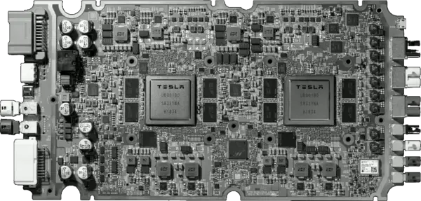
The FSD computer is designed to be retrofitted into existing Tesla models and is therefore largely the same in terms of form factor and I/O. The computer itself fits just behind the glove compartment of the car. The FSD Computer can be installed by a technician in the same slot as the prior Autopilot Hardware 2.5 board. The board itself incorporates two fully independent FSD chips along with their own power subsystem, DRAM, and flash memory for full redundancy. Each chip boots up from its own storage memory and runs its own independent operating system. On the right of the board (shown below) are the eight camera connectors. The power supply and controls are on the left side of the board. The board sits on two independent power supplies - one for one of the FSD chips and one for the other. Additionally, half of the cameras sit on one power supply and the other half sit on the second power supply (note that the video input itself is received by both chips).
The computer itself intakes inputs from a variety of sources including current car readings such as acceleration and speed, radar, GPS, IMU, ultrasonic sensors, wheel ticks, steering angle, and maps data. Data is fed to both FSD chips simultaneously for processing. The two chips independently form a future plan for the car which is then consequently compared between the two chips to ensure an agreement was reached. Once the two plans from both chips agree on the calculated plan, the car can proceed and drive. The drive commands are then validated and sensory information is used as feedback for ensuring the commands executed the desired operations.
Die
SoC
- Samsung 14 nm process
- 12 metal layers
- 260 mm² die size
- ~20 mm x 13 mm die size
- 6,000,000,000 transistors
- 250,000,000 gates
NPU
- 96 x 96 multiply-accumulates
- 9,216 MACs
- 36.864 trillion OPs
- 9,216 MACs @ 2 GHz
- ~47.54 mm²
Top bumps
- Samsung 14 nm process
- 12 metal layers
- 12,464 C4 bumps
See also
- Nvidia Tegra Xavier
- Intel Mobileye EyeQ
Bibliography
- Tesla Autonomy Day, Apr 22, 2019
- Tesla, personal communication, April 25, 2019
| base frequency | 2,200 MHz (2.2 GHz, 2,200,000 kHz) + |
| core count | 12 + |
| core name | Cortex-A72 + |
| core stepping | B0 + |
| designer | Tesla (car company) + |
| die area | 260 mm² (0.403 in², 2.6 cm², 260,000,000 µm²) + |
| die length | 20 mm (2 cm, 0.787 in, 20,000 µm) + |
| die width | 13 mm (1.3 cm, 0.512 in, 13,000 µm) + |
| first announced | April 22, 2019 + |
| first launched | March 10, 2019 + |
| full page name | tesla (car company)/fsd chip + |
| has ecc memory support | true + |
| instance of | microprocessor + |
| isa | ARMv8.0-A + |
| isa family | ARM + |
| ldate | March 10, 2019 + |
| main image |  + + |
| manufacturer | Samsung + |
| market segment | Automotive + |
| max memory bandwidth | 63.58 GiB/s (65,105.92 MiB/s, 68.269 GB/s, 68,268.505 MB/s, 0.0621 TiB/s, 0.0683 TB/s) + |
| max memory channels | 8 + |
| microarchitecture | Cortex-A72 + |
| name | FSD Chip + |
| package | FCBGA-2116 + |
| process | 14 nm (0.014 μm, 1.4e-5 mm) + |
| supported memory type | LPDDR4-4266 + |
| technology | CMOS + |
| thread count | 12 + |
| transistor count | 6,000,000,000 + |
| word size | 64 bit (8 octets, 16 nibbles) + |
