From WikiChip
Difference between revisions of "nervana/microarchitectures/spring crest"
| Line 28: | Line 28: | ||
{{expand list}} | {{expand list}} | ||
| + | |||
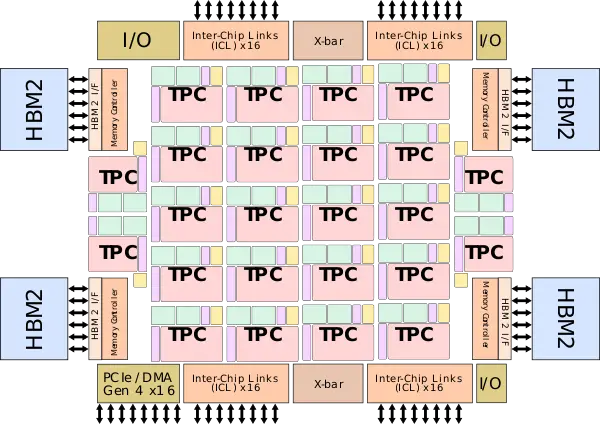
| + | === Block Diagram === | ||
| + | ==== Chip ==== | ||
| + | :[[File:spring crest block diagram.svg|600px]] | ||
== Overview == | == Overview == | ||
Revision as of 20:10, 15 April 2019
| Edit Values | |
| Spring Crest µarch | |
| General Info | |
| Arch Type | NPU |
| Designer | Nervana |
| Manufacturer | Intel |
| Introduction | 2019 |
| Process | 16 nm |
| PE Configs | 24 |
| Succession | |
Spring Crest is the successor to Lake Crest, a planned neural processor microarchitecture designed by Intel Nervana.
Produces based on Spring Crest are branded as the NNP L-1000 series.
Contents
Process Technology
Spring Crest is fabricated on TSMC's 16 nm process.
Architecture
Spring Crest largely builds on the prior generation but introduces more enhancements and compute.
Key changes from Lake Crest
- 16 nm process (from 28 nm)
- 2x computer clusters (24 CCs, up from 12)
- 33% more InterChip Links (16 ICLs, up from 12)
This list is incomplete; you can help by expanding it.
Block Diagram
Chip
Overview
| This section is empty; you can help add the missing info by editing this page. |
Scalability
| This section is empty; you can help add the missing info by editing this page. |
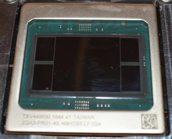
Die
- 16 nm process
- ~741 mm² (estimated)
- ~26 mm x 28.5 mm
Facts about "Spring Crest - Microarchitectures - Intel Nervana"
| codename | Spring Crest + |
| designer | Nervana + |
| first launched | 2019 + |
| full page name | nervana/microarchitectures/spring crest + |
| instance of | microarchitecture + |
| manufacturer | Intel + |
| name | Spring Crest + |
| process | 16 nm (0.016 μm, 1.6e-5 mm) + |
| processing element count | 24 + |

