(→Control) |
(→Memory Hierarchy) |
||
| Line 58: | Line 58: | ||
*** Write-through policy | *** Write-through policy | ||
*** Per core | *** Per core | ||
| − | + | * System DRAM | |
| − | + | ** Up to 64 MiB | |
== Overview == | == Overview == | ||
Revision as of 16:34, 2 July 2017
| Edit Values | |
| ARM3 µarch | |
| General Info | |
| Arch Type | CPU |
| Designer | Acorn Computers |
| Manufacturer | VLSI Technology, Sanyo |
| Introduction | 1989 |
| Process | 1.5 µm |
| Core Configs | 1 |
| Pipeline | |
| Type | Scalar, Pipelined |
| Stages | 3 |
| Decode | 1-way |
| Instructions | |
| ISA | ARMv2a |
| Cache | |
| L1 Cache | 4 KiB/core 64-way set associative |
| Cores | |
| Core Names | ARM3, ARM250 |
| Succession | |
ARM3 is the second-generation commercial ARM implementation designed by Acorn Computers as a successor to the ARM2.
Contents
History
- See also: ARM's History
The ARM3 builds on the success of the ARM2 with higher performance through the introduction of on-die cache but without any major changes to the core itself. The ARM3 was designed by a team of four engineers in nine months and was introduced in 1989. The ARM3 can operate at up to 25 MHz with a peak performance of 25 MIPS and a sustainable performance of 12 MIPS.
Process Technology
- See also: 1.5 µm process
The ARM3 was implemented on a 1.5 µm double-level metal CMOS process.
Architecture
The major goal of the ARM3 was to improve performance. A target of three times the performance of the ARM2 was set. In order to support a faster microprocessor, the system would have to use faster DRAM which would negatively impact the overall cost. Instead, the design team opted to integrating cache.
Key changes from ARM2
- Goal 3x the performance
- Integrated cache
- Integrated clock generator
- Integrated control logic
- Integrated co-processor interface
New instructions
New ARM3 instructions:
Memory:
-
SWP- Swap word memory-register, Atomic (uninterruptible)
Memory Hierarchy
- Cache
- L1 Cache (unified)
- 4 KiB, 64-way set associative
- 16 B line size
- Write-through policy
- Per core
- L1 Cache (unified)
- System DRAM
- Up to 64 MiB
Overview
Control
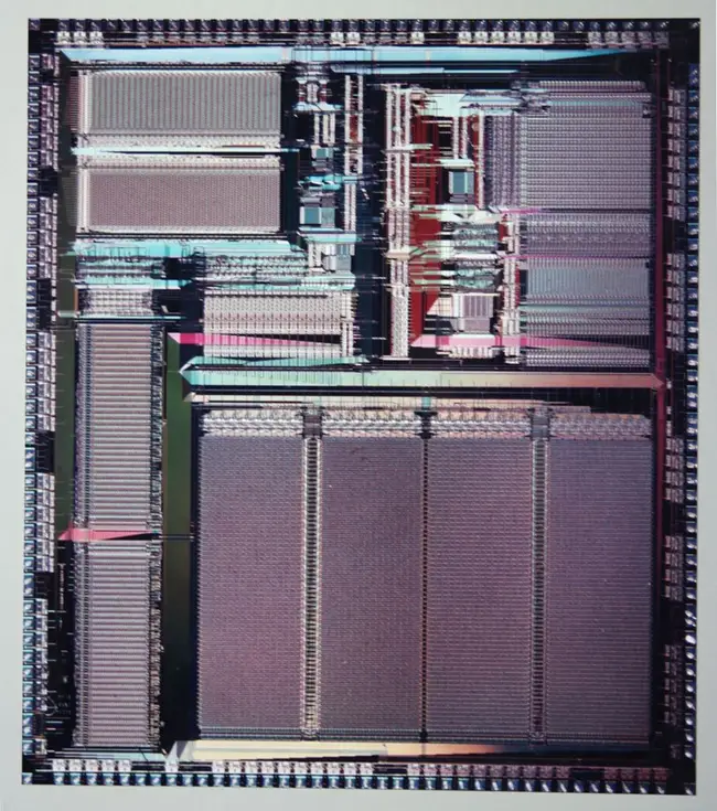
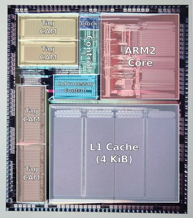
The ARM3's control logic is a state machine implemented as three PLAs. Layout was generated automatically using EDA tools using Psuedo nMOS logic in order to save on space, albeit at the slight expense of static power dissipation.
Core
Pipeline
- Main article: ARM2 Pipeline
ARM3's pipeline is identical to the ARM2.
Clock Generator
| This section is empty; you can help add the missing info by editing this page. |
Coprocessor Interface
| This section is empty; you can help add the missing info by editing this page. |
Cache
| This section is empty; you can help add the missing info by editing this page. |
Die
- 12 MHz, 1 W
- 1.5 µm DLM CMOS
- 8.72 mm x 9.95 mm
- 86.764 mm² die size
- 309,656 transistors
- 206,454 SRAM
- 62,973 CAM
- 40,229 logic
- QFP-160
- 119 signal pins
- 41 power/ground pins
All ARM3 Chips
| List of ARM3-based Processors | ||||||||||||
|---|---|---|---|---|---|---|---|---|---|---|---|---|
| Model | Process | Launched | Frequency | Power Dissipation | Max Memory | |||||||
| VL86C020 | ARM3 | 1989 | 20 MHz 0.02 GHz , 25 MHz20,000 kHz 0.025 GHz , 33 MHz25,000 kHz 0.033 GHz , 36 MHz33,000 kHz 0.036 GHz 36,000 kHz | 2 W 2,000 mW 0.00268 hp 0.002 kW | 64 MiB 65,536 KiB 67,108,864 B 0.0625 GiB 6.103516e-5 TiB | |||||||
| Count: 1 | ||||||||||||
References
- Thomas, A. R. P., et al. "A 2nd Generation 32b RISC Processor with 4KByte Cache." Solid-State Circuits Conference, 1989. ESSCIRC'89. Proceedings of the 15th European. IEEE, 1989.
| codename | ARM3 + |
| core count | 1 + |
| designer | Acorn Computers + |
| first launched | 1989 + |
| full page name | acorn/microarchitectures/arm3 + |
| instance of | microarchitecture + |
| instruction set architecture | ARMv2a + |
| manufacturer | VLSI Technology + and Sanyo + |
| microarchitecture type | CPU + |
| name | ARM3 + |
| pipeline stages | 3 + |
| process | 1,500 nm (1.5 μm, 0.0015 mm) + |

