(Created page with "{{amd title|Socket sTRX4}} {{package |name=Socket sTRX4 |designer=AMD |market=HEDT |first launched=November 25, 2019 |microarch=Zen 2 |tdp=280 W |package name=sTRX4 |package n...") |
|||
| (One intermediate revision by one other user not shown) | |||
| Line 1: | Line 1: | ||
{{amd title|Socket sTRX4}} | {{amd title|Socket sTRX4}} | ||
{{package | {{package | ||
| − | |name= | + | |name=ryzen 5 1600 |
|designer=AMD | |designer=AMD | ||
| + | |first launched=November 25, 2019 | ||
|market=HEDT | |market=HEDT | ||
| − | |||
|microarch=Zen 2 | |microarch=Zen 2 | ||
|tdp=280 W | |tdp=280 W | ||
| Line 14: | Line 14: | ||
|package dimension 2=58.50 mm | |package dimension 2=58.50 mm | ||
|package dimension 3=6.26 mm | |package dimension 3=6.26 mm | ||
| − | |pitch=0.87 mm | + | |package pitch=0.87 mm |
| − | |pitch 2=1.00 mm | + | |package pitch 2=1.00 mm |
| + | |socket name=sTRX4 | ||
|socket type=SM-LGA | |socket type=SM-LGA | ||
| − | |||
|predecessor=Socket TR4 | |predecessor=Socket TR4 | ||
|predecessor link=amd/packages/socket tr4 | |predecessor link=amd/packages/socket tr4 | ||
Latest revision as of 10:45, 6 April 2024
| Edit Values | |
| ryzen 5 1600 | |
| General Info | |
| Designer | AMD |
| Introduction | November 25, 2019 (launched) |
| Market | HEDT |
| Microarchitecture | Zen 2 |
| TDP | 280 W 280,000 mW 0.375 hp 0.28 kW |
| Package | |
| Name | sTRX4, FCLGA-4094 |
| Type | FC-OLGA |
| Contacts | 4094 |
| Dimension | 75.40 mm 7.54 cm × 58.50 mm2.969 in 5.85 cm × 6.26 mm2.303 in 0.246 in |
| Pitch | 0.87 mm 0.0343 in × 1.00 mm0.0394 in |
| Socket | |
| Name | sTRX4 |
| Type | SM-LGA |
| Succession | |
| Contemporary | |
| Socket sWRX8 Socket SP3 | |
Socket sTRX4 is a microprocessor socket designed by AMD for their third generation Ryzen Threadripper high end desktop processors, the successor to Socket TR4. Contemporary mainstream desktop, workstation, and server processors use Socket AM4, sWRX8, and SP3 respectively.
Socket sTRX4 is mechanically identical and almost pin-compatible to Socket SP3 and the sockets TR4 and sWRX8 also derived from it, but differs by the number of memory channels and I/O interfaces available: SP3 processors use DDR4 RDIMMs on up to eight memory channels, sWRX8 processors UDIMMs or RDIMMs, while TR4 and sTRX4 processors support only UDIMMs on up to four memory channels. TR4 and sTRX4 omit four of eight PCIe interfaces present on Socket SP3 and sWRX8, but TR4 processors also pin out four additional USB ports and a HDA interface which are not supported by the other infrastructures.
While sTRX4 processors were designed to be backwards compatible with Socket TR4 they are not supported on first generation Threadripper motherboards, nor are TR4 processors accepted on sTRX4 boards. sTRX4 processors are also not supported in Socket SP3 and sWRX8 or vice versa.
Contents
Overview[edit]
Socket sTRX4 is a zero insertion force, screw actuated, surface-mount land grid array socket for use with a 4094-contact, 1.00 mm × 0.87 mm interstitial pitch, organic land grid array CPU package.
This single socket client infrastructure supports four channels of 72-bit DDR4 memory with up to two UDIMMs per channel, four 16-lane PCIe Gen 4 I/O links, four USB 3.2 Gen 2 ports, and up to 16 SATA Gen 3 ports. 8-layer motherboards are required to route these signals.
The following AMD processor families use Socket sTRX4:
| CPU Family | Microarch. | Process | Products | |
|---|---|---|---|---|
| Type 1 | Family 17h Models 30h–3Fh | Zen 2 | 7 nm & 12 nm | Ryzen Threadripper 3900 "Castle Peak" (Model 31h) |
| Type 2 | Family 19h Models 00h–0Fh | Zen 3 | 7 nm & 12 nm(?) |
The codename of AMD's sTRX4 reference platform (CRB) is "Sharkstooth".
Package Description[edit]
The sTRX4 CPU package is lidded, has a 58.50 mm × 75.40 mm organic substrate with flip chip die attachment, and 4094 nickel and gold plated land pads. It ships with a carrier frame pre-installed. The carrier frame, made from an orange colored polycarbonate material, is a part of the package loading mechanism and remains on the package in the socket.
The package substrate has six keying notches along the short edges preventing it from being inserted 180 degrees rotated into the carrier frame or socket, or in an incompatible socket with mismatching keying features. Four additional positions are reserved for future models. However all sockets SP3, TR4, sTRX4, and sWRX8, and all processors for these sockets have the same keying. It is worth noting that these processors are also electrically keyed by pin SP3R1 and SP3R2. To boot the processor the motherboard must also provide compatible firmware. A triangular symbol on both sides of the substrate marks the location of pin A1, with corresponding markings on the socket. Decoupling capacitors are placed under the lid around the chiplets on the top side, and in two windows in the pad grid on the bottom side.
sTRX4 is a multi-chip package integrating one I/O die and 4 or 8 Core Complex Dies which contain eight CPU cores each. The CCDs closer to the IOD are populated first. The I/O die contains eight memory controllers, eight 16-lane multi-function I/O interfaces, and other I/O facilities. The silicon in sTRX4 processors is "Starship" rev. SSP-B0. AMD used the same chips for EPYC 7002 server and embedded processors, and Ryzen Threadripper workstation processors; see CPU Family 17h.
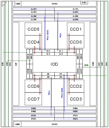
The diagram on the left (top view, not to scale) shows the routing of high speed signals between the dies and the package contacts. Eight CCM blocks extend the Data Fabric on the IOD to the CCDs, each driving a GMI2 physical link routed on two package layers. AMD chose not to route these signals on a 2.5D interposer or EMIB for reasons of product flexibility and reach. SSP-B0 CCDs contain two CCXs with 16 MiB L3 cache each, the GMI2 port and its die bumps are located in the center of the die to reduce memory latency from the L3 cache. GMI2 links are serial, single-ended links with 31 transmit (to IOD) and 39 receive lanes, one clock gating lane per direction, and a differential pair of clock lanes. They use customized 10:1 SerDes running at FCLK, so for instance a 1.46 GHz FCLK coupled to the bus clock of DDR4-2933 SDRAM gives a raw data rate of 14.6 GT/s per lane or 71.2 GB/s per link from IOD to CCD. Not shown are eight TWIX ports which extend the Control Fabric to the CCDs, these links run on four data and two clock lanes, as well as USB signals and low speed busses. For details and the IOD internal topology see AMD Infinity Fabric.sTRX4 packages are not merely reconfigured EPYC processors, they support memory and I/O interfaces on the same pins as Socket TR4 processors and the signal routing on the package differs from Socket SP3 and sWRX8 packages in the following ways:
- Only four of the eight DRAM channels A-H are usable, namely A, D, E, and H, connected to UMC2, 3, 4, and 5 on the IOD. UDIMMs are supported, but not RDIMMs. Memory up to DDR4-3200 (not overclocked) is supported, TR4 processors are rated for up to DDR4-2933 memory.
- Only four of the eight 16-lane I/O interfaces P0-P3 and G0-G3 are usable, namely P0, P2, G0, and G2, connected to SerDes P1, P3, G1, and G2 on the IOD. All of these I/O interfaces can be configured as PCIe link, some lanes alternatively as SATA link. The xGMI, S-Link, and XGBE protocols are not supported on this socket. (The cache coherent xGMI links connect the Data Fabrics of each processor on dual socket systems. S-Link is a cache coherent link to CCIX memory expanders. XGBE is a backplane Ethernet link with data rates up to 10 Gbit/s.) TR4 processors do not support PCIe Gen 4.
- SATA is an alternative function on the P0, P1, G2, and G3 interfaces so only 16 of the 32 SATA links are usable.
- The WAFL interface is not supported on this socket, or on Socket TR4 or sWRX8.
Socket Description[edit]
Socket sTRX4 is mechanically identical to Socket SP3.
Features[edit]
- Lidded land grid array package, 75.40 mm × 58.50 mm
- 4094 contacts in a 82 × 55 grid with 0.87 mm × 1.00 mm interstitial pitch
- Organic substrate, flip chip die attachment
- 4 × 64/72 bit DDR4 SDRAM interface
- Up to 1600 MHz, PC4-25600 (DDR4-3200), 102.4 GB/s total raw bandwidth, not overclocked
- Up to 2 DIMMs/channel, up to 8 DIMMs total
- SR/DR UDIMM types only
- ECC supported
- Memory addressing up to 1 TiB/channel
- Max. total memory capacity 256 GiB using eight 32 GiB DIMMs
- Four multi-function I/O interfaces P0, P2, G0, G2
Lane 15 14 13 12 11 10 9 8 7 6 5 4 3 2 1 0 PCIe x16 x8 x8 x4 x4 x4 x4 x2 x2 x2 x2 x2 x2 x2 x2 x1 x1 x1 x1 x1 x1 x1 x1 x1 x1 x1 x1 x1 x1 x1 x1 SATA 7 6 5 4 3 2 1 0 PHY 3 PHY 2 PHY 1 PHY 0
- PCIe Gen 1, 2, 3, 4 (16 GT/s) protocol supported on P0, P2, G0, G2
- 16 lanes, up to 8 ports per interface configurable x16, x8, x4, x2, x1 with power-of-two alignment (e.g. 1x4 + 4x1 + 1x8)
- Max. 7 PCIe ports in each 8-lane subset (e.g. 0x8 + 8x1 is not possible)
- Max. 7 PCIe ports per interface if any lane is configured as SATA port
- Different PCIe generations supported on the ports in the same interface
- Lane polarity inversion, per port lane reversal
- Up to 56 PCIe lanes total (one x8 link reserved for chipset attachment)
- PCIe Gen 1, 2, 3, 4 (16 GT/s) protocol supported on P0, P2, G0, G2
- SATA Gen 1, 2, 3 (6 Gb/s) protocol supported on the lower 8 lanes of P0 and G2
- P0: SATA00-07, G2: SATA20-27
- Up to 16 SATA ports total
- SATA Gen 1, 2, 3 (6 Gb/s) protocol supported on the lower 8 lanes of P0 and G2
- Four PHY groups on each interface
- Lanes sharing a PHY group must use the same protocol (PCIe, SATA)
- Four PHY groups on each interface
- 4 × USB 1.1, 2.0, 3.2 Gen 2×1 (10 Gb/s) ports
- Type-C connectors are supported with external components
- Low speed interfaces (some sharing pins):
Chipsets[edit]
sTRX4 processors are SoCs with an integrated controller hub so they do not require a chipset, but are paired with the AMD TRX40 chipset (AMD 500-Series) serving as I/O expander.
The chipset is attached with an x8 PCIe link and can provide the following additional interfaces:
- 16 lanes (+ 8-lane CPU link) PCIe Gen 1, 2, 3, 4 (16 GT/s)
- 8 × SATA Gen 1, 2, 3 (6 Gb/s) ports sharing pins with the PCIe interface
- 4 × SATA Gen 1, 2, 3 (6 Gb/s) ports, dedicated
- 8 × USB 1.1, 2.0, 3.2 Gen 2 (10 Gb/s) ports
- 5 × USB 1.1, 2.0 ports
An audio interface is not provided by Socket sTRX4 or the chipset, an audio controller is commonly attached as on-board USB device. The sTRX4/TRX40 platform supports overclocking.
Processors using Socket sTRX4[edit]
| Model | Family | Microarch. | Cores | Threads | L2$ | L3$ | Base | Turbo | Memory | TDP | Launched | Price | OPN |
|---|---|---|---|---|---|---|---|---|---|---|---|---|---|
| 3960X | Ryzen Threadripper | Zen 2 | 24 | 48 | 12 MiB 12,288 KiB 12,582,912 B 0.0117 GiB | 128 MiB 131,072 KiB 134,217,728 B 0.125 GiB | 3.8 GHz 3,800 MHz 3,800,000 kHz | 4.5 GHz 4,500 MHz 4,500,000 kHz | DDR4-3200 | 280 W 280,000 mW 0.375 hp 0.28 kW | 25 November 2019 | $ 1,399.00 € 1,259.10 £ 1,133.19 ¥ 144,558.67 | 100-000000010, 100-100000010WOF |
| 3970X | Ryzen Threadripper | Zen 2 | 32 | 64 | 16 MiB 16,384 KiB 16,777,216 B 0.0156 GiB | 128 MiB 131,072 KiB 134,217,728 B 0.125 GiB | 3.7 GHz 3,700 MHz 3,700,000 kHz | 4.5 GHz 4,500 MHz 4,500,000 kHz | DDR4-3200 | 280 W 280,000 mW 0.375 hp 0.28 kW | 25 November 2019 | $ 1,999.00 € 1,799.10 £ 1,619.19 ¥ 206,556.67 | 100-000000011, 100-100000011WOF |
| 3980X | Ryzen Threadripper | Zen 2 | 48 | 96 | 24 MiB 24,576 KiB 25,165,824 B 0.0234 GiB | 3.2 GHz 3,200 MHz 3,200,000 kHz | 4.5 GHz 4,500 MHz 4,500,000 kHz | DDR4-3200 | 280 W 280,000 mW 0.375 hp 0.28 kW | ||||
| 3990X | Ryzen Threadripper | Zen 2 | 64 | 128 | 32 MiB 32,768 KiB 33,554,432 B 0.0313 GiB | 256 MiB 262,144 KiB 268,435,456 B 0.25 GiB | 2.9 GHz 2,900 MHz 2,900,000 kHz | 4.3 GHz 4,300 MHz 4,300,000 kHz | DDR4-3200 | 280 W 280,000 mW 0.375 hp 0.28 kW | 7 February 2020 | $ 3,990.00 € 3,591.00 £ 3,231.90 ¥ 412,286.70 | 100-000000163, 100-100000163WOF |
| Count: 4 |
Photos[edit]
| This section is empty; you can help add the missing info by editing this page. |
Package Diagram[edit]
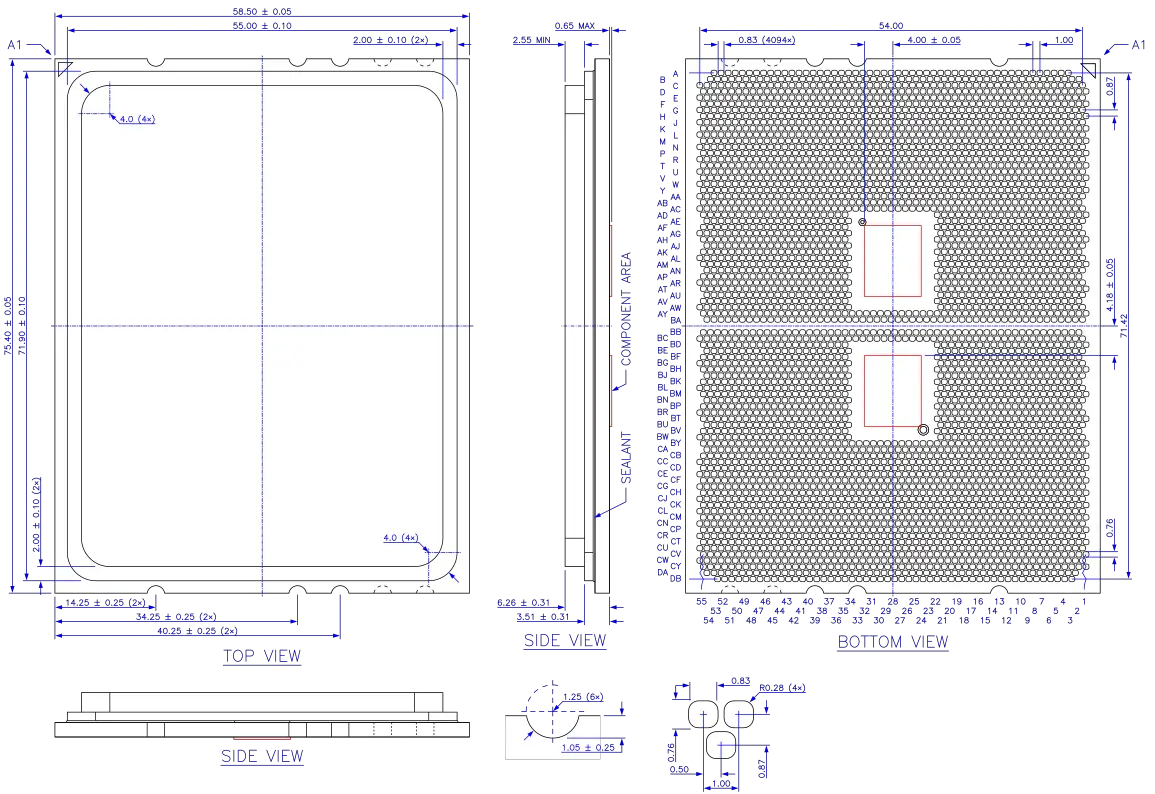
sTRX4 package (same as Socket SP3 package). All dimensions in millimeters.
Socket Diagrams[edit]
Pin Map[edit]
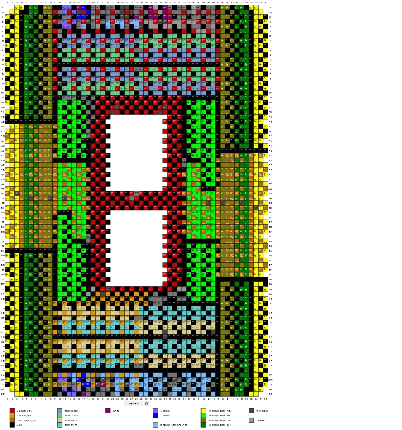
Socket sTRX4 pinout (same as Socket SP3, with some constraints), top view. This is a preview, click for a larger image and other views.
Pin Description[edit]
See Socket SP3.
Bibliography[edit]
- "Socket SP3 Design Specification", AMD Publ. #55260, Rev. 1.16, August 2020
- "Functional Data Sheet for sTRX4 and sWRX8 Processors", AMD Publ. #56515, Rev. 0.81, August 2019
- "Infrastructure Roadmap for sTRX4 and sWRX8 Processors", AMD Publ. #56443, Rev. 0.92, July 2021
- "Preliminary Processor Programming Reference (PPR) for AMD Family 17h Model 31h, Revision B0 Processors", AMD Publ. #55803, Rev. 0.93, October 28, 2020
- "Revision Guide for AMD Family 17h Models 30h-3Fh Processors", AMD Publ. #56323, Rev. 0.78, February 2021
- Burd, Thomas et al. (2018). “Zeppelin”: An SoC for Multichip Architectures. IEEE JSSC. 54 (1): 133-143. doi:10.1109/JSSC.2018.2873584
- Singh, Teja et al. (2020). Zen 2: The AMD 7nm Energy-Efficient High-Performance x86-64 Microprocessor Core. Proceedings of IEEE ISSCC 2020. pp. 42-44. doi:10.1109/ISSCC19947.2020.9063113
- Naffziger, Samuel; Lepak, Kevin; Paraschou, Milam; Subramony, Mahesh (2020). AMD Chiplet Architecture for High-Performance Server and Desktop Products. Proceedings of IEEE ISSCC 2020. pp. 44-45. doi:10.1109/ISSCC19947.2020.9063103
- Naffziger, Samuel. "AMD Chiplet Architecture for High-Performance Server and Desktop Products", IEEE ISSCC 2020, February 17, 2020
See also[edit]
| designer | AMD + |
| first launched | November 25, 2019 + |
| instance of | package + |
| market segment | HEDT + |
| microarchitecture | Zen 2 + |
| name | ryzen 5 1600 + |
| package | sTRX4 + and FCLGA-4094 + |
| package contacts | 4,094 + |
| package height | 6.26 mm (0.246 in) + |
| package length | 75.4 mm (7.54 cm, 2.969 in) + |
| package pitch | 0.87 mm (0.0343 in) + and 1 mm (0.0394 in) + |
| package type | FC-OLGA + |
| package width | 58.5 mm (5.85 cm, 2.303 in) + |
| socket | sTRX4 + |
| tdp | 280 W (280,000 mW, 0.375 hp, 0.28 kW) + |


