(Added package info.) |
|||
| (34 intermediate revisions by 7 users not shown) | |||
| Line 1: | Line 1: | ||
{{microsoft title|Scorpio Engine}} | {{microsoft title|Scorpio Engine}} | ||
| − | {{ | + | {{chip |
|name=Scorpio Engine | |name=Scorpio Engine | ||
|image=scorpio engine (front).png | |image=scorpio engine (front).png | ||
| Line 11: | Line 11: | ||
|first launched=November 7, 2017 | |first launched=November 7, 2017 | ||
|frequency=2,300 MHz | |frequency=2,300 MHz | ||
| − | |||
|isa=x86-64 | |isa=x86-64 | ||
|isa family=x86 | |isa family=x86 | ||
|microarch=Enhanced Jaguar | |microarch=Enhanced Jaguar | ||
| − | |microarch 2= | + | |microarch 2=Polaris |
|core name=Enhanced Jaguar | |core name=Enhanced Jaguar | ||
|process=16 nm | |process=16 nm | ||
| Line 21: | Line 20: | ||
|technology=CMOS | |technology=CMOS | ||
|die area=359 mm² | |die area=359 mm² | ||
| + | |mcp=No | ||
|word size=64 bit | |word size=64 bit | ||
|core count=8 | |core count=8 | ||
|thread count=8 | |thread count=8 | ||
|max cpus=1 | |max cpus=1 | ||
| − | |max memory= | + | |max memory=24 GiB |
| + | |package name=amd/packages/bga-2409 | ||
}} | }} | ||
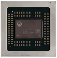
'''Scorpio Engine''' is a {{arch|64}} [[octa-core]] [[x86]] SoC designed by [[AMD]] and [[Microsoft]] for their ''Xbox One X''. The chip features eight {{amd|Enhanced Jaguar|l=arch}} cores operating at 2.3 GHz and a custom {{amd|Arctic Islands|l=arch}}-based GPU operating at 1.172 GHz. Fabricated on [[TSMC]]'s [[16 nm process|16FF+]], this chip supports 12 (24 for Dev) GiB of 12-channel GDDR5-6800 memory. | '''Scorpio Engine''' is a {{arch|64}} [[octa-core]] [[x86]] SoC designed by [[AMD]] and [[Microsoft]] for their ''Xbox One X''. The chip features eight {{amd|Enhanced Jaguar|l=arch}} cores operating at 2.3 GHz and a custom {{amd|Arctic Islands|l=arch}}-based GPU operating at 1.172 GHz. Fabricated on [[TSMC]]'s [[16 nm process|16FF+]], this chip supports 12 (24 for Dev) GiB of 12-channel GDDR5-6800 memory. | ||
| + | |||
| + | == Overview == | ||
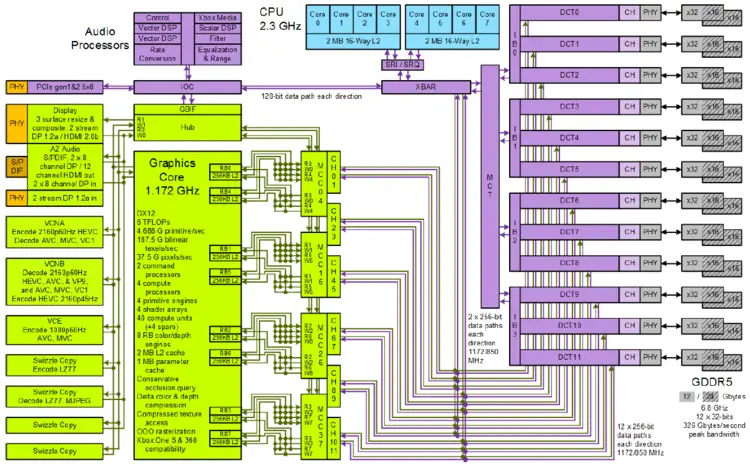
| + | Like the ''PlayStation 4'' and the ''Xbox One'', the ''Xbox One X'' is also powered by a chip based on [[AMD]]'s architectures. The ''Scorpio Engine'' most important goal was achieving true [[4K]] gaming performance according to John Sell, a Distinguished Engineer at Microsoft who presented the chip at [[Hot Chips]] 29. Fabricated on [[TSMC]]'s [[16 nm process]], the chip contains 7 billion [[transistors]] on a 359 mm² [[die]], similar in amount to [[Nvidia]]'s {{nvidia|GTX 1080}} and almost the same size as the original Xbox One SoC (which was 363 mm² on a [[28 nm process]]). | ||
| + | |||
| + | Like the original Xbox One SoC, the chip feature eight Jaguar cores. The cores have been {{amd|Enhanced Jaguar|lightly enhanced|l=arch}} and operate at a higher frequency of 2.3 GHz, but are otherwise mostly identical. It's worth pointing out that [[AMD]] has not commercialized a 16 nm Jaguar processor outside of this chip. | ||
| + | |||
| + | |||
| + | :[[File:scorpio engine block diagram.png|750px]] | ||
== Cache == | == Cache == | ||
| Line 47: | Line 56: | ||
== Memory controller == | == Memory controller == | ||
| + | The memory architecture of the Scorpio Engine is very different from the previous generational chip. The entire memory subsystem was redesigned to address the major deficiencies in prior chips. In previous chip, Microsoft chose to go with 8 GiB of quad-channel [[DDR3]] on-board operating at 2133 MT/s for a total system memory [[bandwidth]] of 63.58 GiB/s. That was fairly low by any standard; at the time the PS4 SoC had a peak memory bandwidth of 163.9 GiB/s. In an attempt to mitigate the lack of bandwidth, the chip incorporated 32 MiB of [[eSRAM]] with a bus of 1,024-bit in each direction for a total bandwidth of 190 GiB/s. While this reduced the cost of memory considerably, it increased the cost in terms of die area (which would be roughly 1.6B transistors). Additionally, this architecture also made the programming model more complicated to work with. | ||
| + | |||
| + | The Scorpio Engine made a 180-degree turn vs previous chip architecture-wise. The entire memory subsystem has been re-designed with GDDR5 and high bandwidth in mind. The previous 32 MiB of [[eSRAM]] has been eliminated. Instead, Scorpio has a maximum bandwidth of 304 GiB/s through a 384-bit wide [[DRAM]] interface with an effective transfer of 6800 MT/s. The bandwidth increase has effectively reached the level of a discrete graphics card and almost 1.5x the bandwidth of the PS4 Pro (which is 203 GiB/s). | ||
| + | |||
| + | Console systems will come with 12 x32 [[GDDR]] chips for a total of 12 [[GiB]] while the development system will come with x16 chips for a total capacity of 24 GiB. Scorpio has 12 [[DRAM controllers]] for each of the 12 channels. It's worth noting that in order to maintain backwards compatibility with the Xbox One software, the [[CPU]] and [[GPU]] accesses the memory separately. The exact details of how the CPU accesses the memory has not been detailed. As with the previous generation, a bidirectional bus sits between the [[memory controllers]] and the CPUs and GPU. The bus maintains [[coherency]] between the CPU cores and the GPU. For the GPU, each of the 12 [[memory channel|channels]] is a 256-bit directional bus for a total bus width of 3,072-bit. The 12 channels allow the system to lower the granularity of memory accesses while the wide bus allows the system to take full advantage of the available bandwidth. | ||
| + | |||
{{memory controller | {{memory controller | ||
|type=GDDR5-6800 | |type=GDDR5-6800 | ||
| − | |max mem= | + | |ecc=No |
| + | |max mem=24 GiB | ||
|controllers=12 | |controllers=12 | ||
|channels=12 | |channels=12 | ||
| Line 58: | Line 74: | ||
== Graphics == | == Graphics == | ||
| − | {{ | + | {{further|amd/microarchitectures/arctic islands|l1=Arctic Islands microarchitecture}} |
| − | + | {| class="wikitable" style="float: right;" | |
| − | |||
| − | |||
| − | |||
| − | |||
| − | |||
| − | |||
| − | |||
| − | |||
| − | |||
| − | |||
! colspan="3" | Hardware Accelerated Video Capabilities | ! colspan="3" | Hardware Accelerated Video Capabilities | ||
|- | |- | ||
| Line 80: | Line 86: | ||
| [[VP9]] || {{tchk|yes|4K @ 60 Hz}} || {{tchk|no}} | | [[VP9]] || {{tchk|yes|4K @ 60 Hz}} || {{tchk|no}} | ||
|} | |} | ||
| + | Scorpio Engine feature 40 or 44 Compute Units (CUs) for the consumer console and dev kit respectively based on {{amd|Arctic Islands|l=arch}} (Similar to Polaris, Radeon RX 4xx). This is triple the amount over the original Xbox One SoC. The Compute Units operate at 1,172 MHz, each with 64 32-bit [[floating point]] [[multiply-accumulate]] units. At 1.172 GHz with 128 FLOP/cycle this chip can deliver 6.00064 [[TFLOPS]] raw peak performance - over four times previous chips (which were 1.3 and 1.4 TFLOPS). The dev kit can deliver a reported 6.6 TFLOPS with its four additional CUs. The performance of texture processing has also been increased to 187.5 G bilinear [[texels]]/second. Additionally, in each of the four [[shader]] arrays, there is one geometry engine for the purpose of doing fixed geometry processing, this is twice previous chip which is capable of 4.688 Giga primitives/second. | ||
| + | |||
| + | Similar to previous chips, Scorpio has 2 command processors (i.e., microcontrollers) that handle graphic and compute tasks however they are said to handle more parallel compute tasks than previous chip in order to increase performance. The number of ACEs (Asynchronous Compute Engine) on Scorpio has doubled to 4 in order to increase the [[parallelism]] possible. It's worth pointing out that since the Scorpio Engine is based on {{amd|Arctic Islands|l=arch}}, there are also two additional schedulers. | ||
| + | |||
| + | [[File:scorpio engine rb-mem subsys.svg|right|400px]] | ||
| + | <table class="wikitable"> | ||
| + | <tr><th colspan="2">Scorpio Engine GPU</th></tr> | ||
| + | <tr><th>Unified shaders</th><td>2560 (64 × 40 CUs), (dev kit) 2816 (64 × 44 CUs)</td></tr> | ||
| + | <tr><th>[[raster operation units|ROPs]]</th><td>32</td></tr> | ||
| + | <tr><th>[[texture mapping units |TMUs]]</th><td>160</td></tr> | ||
| + | <tr><th>Peak Performance</th><td> ~6 TFLOPS (6,000,640,000,000 [[FLOPS]]), (dev kit) ~6.6 TFLOPS</td></tr> | ||
| + | </table> | ||
| + | |||
| + | === RBs and Memory Subsystem === | ||
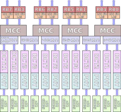
| + | The render back-end has also been enhanced. The render back-end consist of eight ''Render Boxes'' (RB) color/depth engines, each with 256 KiB graphics L2 cache for a total of 2 MiB. Each pair of Render Boxes is wired to one ''Memory Controller Cluster'' (MCC). Each MMC consists of two dedicated memory controllers and two more that are shared between two pairs of MCCs. In total there are four clusters with each having two dedicated controllers and two more pair (4 controllers) of channels shared between a pair of MCCs for a total of 12 channels. | ||
| + | |||
| + | {{clear}} | ||
== Display == | == Display == | ||
| Line 88: | Line 111: | ||
== Utilizing devices == | == Utilizing devices == | ||
| − | + | The Scorpio Engine is used solely in the [[used by::Xbox One X]] and its dev kit. | |
| − | |||
| − | |||
== Die == | == Die == | ||
| Line 102: | Line 123: | ||
: [[File:scorpio engine die shot (annotated).png|750px]] | : [[File:scorpio engine die shot (annotated).png|750px]] | ||
| + | |||
| + | === Yield & redundancy === | ||
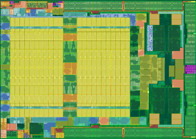
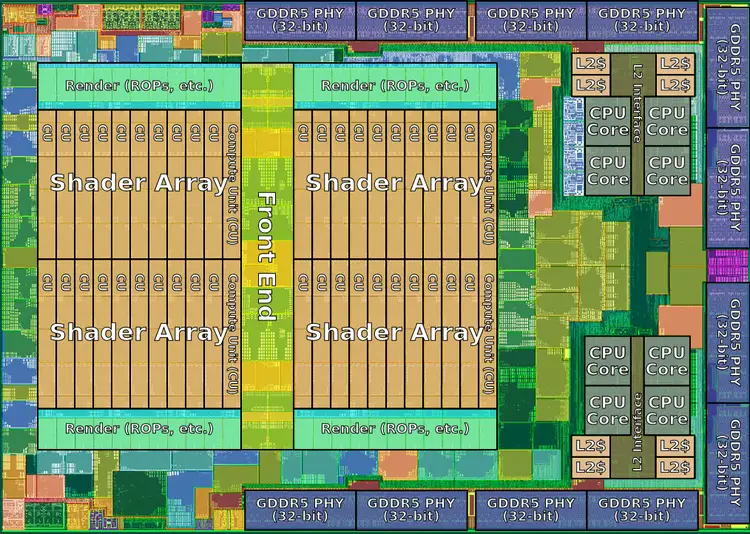
| + | In normal microprocessors such as typical [[CPU]]s and [[GPU]]s, when a core in the case of a CPU or a shader unit in the case of a GPU has a defect, it's common for manufacturers to disable those affected cores/shaders (typically in a symmetrical way) and [[binning|sell those chips as lower end models]]. Since the Scorpio Engine is only found in the single-specification ''Xbox One X'' machine and its dev kit, [[binning]] is not as flexible. In an attempt to improve yield for the consumer models the Scorpio Engine actually incorporates 11 Compute Units (CUs) in each shader array for redundancy, 10 of them are operational while an 11th one is used as a spare. With 4 shader arrays, there are 4 spares and 40 enabled CUs. If one or a few compute units are faulty but the rest of the chip is fully functional, the spare CUs can be enabled to compensate for this. Fully unlocked Scorpio Engines are incorporated in the dev kits, though in lower volume than the consumer models. | ||
| + | |||
| + | == Package == | ||
| + | [[Category:all ic packages]]{{#set:package=BGA-2409|package type=FC-OBGA}} | ||
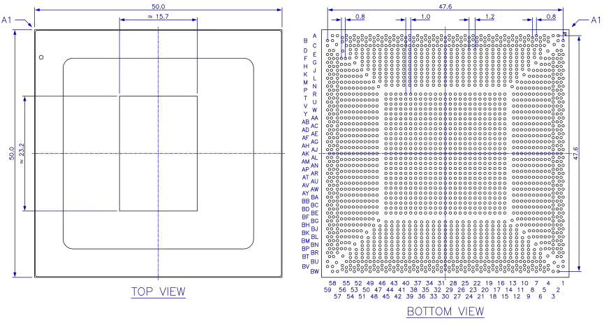
| + | * Lidless [[ball grid array]] package with stiffener frame, [[package length::50 mm]] × [[package width::50 mm]] | ||
| + | ** [[package contacts::2409]] balls, [[package pitch::0.8 mm]] minimum non-uniform pitch | ||
| + | ** 12 layer (5-2-5)<!--ISSCC2021-XSX Paternoster--> organic substrate, [[flip chip]] die attachment | ||
| + | |||
| + | * 12 × 32 bit GDDR5 SDRAM interface | ||
| + | ** 850 MHz, 6800 MT/s, 326.4 GB/s total raw bandwidth | ||
| + | ** XBox consumer model: 1 × DRAM Down per channel, 256M×32 = 1 GiB | ||
| + | |||
| + | * 8-lane PCIe Gen 1, 2, 3 (8 GT/s) interface | ||
| + | ** Up to 5 ports configurable x4, x2, x1 with power-of-two alignment | ||
| + | ** x4 General Purpose Ports (x4 SSD M.2) | ||
| + | ** x4 Unified Media Interface (x2 South Bridge, x1 Ethernet, x1 spare) | ||
| + | |||
| + | * Display Port 0 | ||
| + | ** {{abbr|DP}} 1.2a with 2-stream {{abbr|MST}}, {{abbr|HDMI}} 2.0b, {{abbr|HDCP}} 2.2 | ||
| + | ** Resolution up to 4096 × 2160, 60 Hz | ||
| + | |||
| + | * Display Port 1 | ||
| + | ** DP 1.2a input (lanes 0-1 used for HDMI passthrough via HDMI-DP converter in SB) | ||
| + | |||
| + | * Low speed interfaces: | ||
| + | ** {{abbr|S/PDIF}} output ({{wp|TOSLINK}} connector) | ||
| + | ** {{abbr|GPIO}} | ||
| + | ** Sideband Interface ({{abbr|SB-TSI}}) | ||
| + | ** Serial VID Interface ({{amd|SVI2}}) | ||
| + | ** {{abbr|JTAG}} | ||
| + | |||
| + | === Package Diagram === | ||
| + | [[File:BGA-2409 diag.svg]] | ||
| + | |||
| + | All dimensions in millimeters. | ||
| + | |||
| + | [[:File:BGA-2409 pn.svg|Ball numbers]] | ||
| + | |||
| + | === Pin Map === | ||
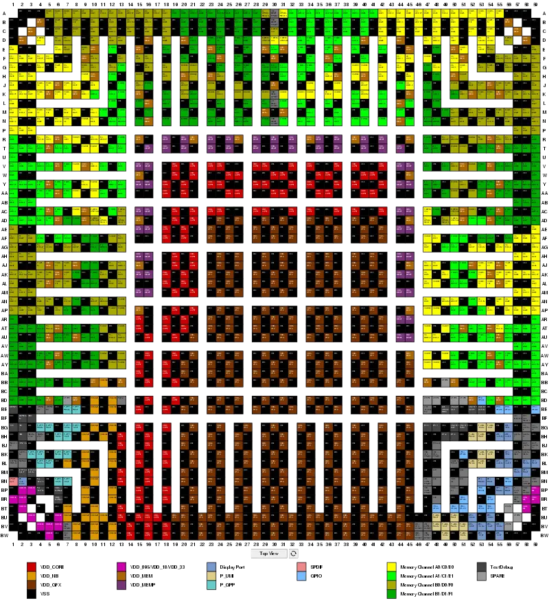
| + | [[File:BGA-2409 pinmap.svg|800px]] | ||
| + | |||
| + | Pinout, top view. Click for a larger image and other views. | ||
| + | |||
| + | [[:File:BGA-2409 pinout.ods|Spreadsheet]] | ||
| + | |||
| + | ==== Pin Description ==== | ||
| + | Signals with names ending in _N are active low. | ||
| + | |||
| + | {| class="wikitable sortable" | ||
| + | ! Signal !! Description | ||
| + | |- | ||
| + | | (A0-F0/A1-F1)_ADBI || DRAM Channel A-F, Subchannel 0-1 Address Bus Inversion | ||
| + | |- | ||
| + | | (A0-F0/A1-F1)_CAS_N || DRAM Column Address Strobe | ||
| + | |- | ||
| + | | (A0-F0/A1-F1)_CKE0 || DRAM Clock Enable for Address/Command Bus | ||
| + | |- | ||
| + | | (A0-F0/A1-F1)_CLK0_P/N || DRAM Differential Clock for Address/Command Bus | ||
| + | |- | ||
| + | | (A0-F0/A1-F1)_CS0_N || DRAM Chip Select | ||
| + | |- | ||
| + | | (A0-F0/A1-F1)_DDBI_(0-3) || DRAM Data Bus Inversion, byte 0-3 | ||
| + | |- | ||
| + | | (A0-F0/A1-F1)_DQ[31:0] || DRAM Data Bus | ||
| + | |- | ||
| + | | A-F_DRAM_RESET || DRAM Reset | ||
| + | |- | ||
| + | | (A0-F0/A1-F1)_EDC_(0-3) || DRAM Error Detection and Correction, Data Bus byte 0-3 | ||
| + | |- | ||
| + | | (A0-F0/A1-F1)_MA_A[7:0] || DRAM Column/Row Address | ||
| + | |- | ||
| + | | (A0-F0/A1-F1)_MA_A12 || DRAM Column/Row Address 12 | ||
| + | |- | ||
| + | | A-F_MEM_CAL || | ||
| + | |- | ||
| + | | A-F_MEM_VREFDQ || DRAM Input Reference for Data Bus | ||
| + | |- | ||
| + | | (A0-F0/A1-F1)_RAS_N || DRAM Row Address Strobe | ||
| + | |- | ||
| + | | (A0-F0/A1-F1)_WCK0/WCK1_P/N || DRAM Differential Forward Clock for Data Bus byte 0-1/2-3 | ||
| + | |- | ||
| + | | (A0-F0/A1-F1)_WE_N || DRAM Write Enable | ||
| + | |- | ||
| + | | P_GPP_RX(0-3)_P/N || PCIe {{abbr|GPP}} Receive Data Differential Pairs | ||
| + | |- | ||
| + | | P_GPP_TX(0-3)_P/N || PCIe GPP Transmit Data Differential Pairs | ||
| + | |- | ||
| + | | P_UMI_RX(0-3)_P/N || PCIe {{abbr|UMI}} Receive Data Differential Pairs | ||
| + | |- | ||
| + | | P_UMI_TX(0-3)_P/N || PCIe UMI Transmit Data Differential Pairs | ||
| + | |- | ||
| + | | DP0_TX(0-3)_P/N || {{wp|DisplayPort}} 0 Main Link Differential Transmitter Lane 0-3 or {{abbr|HDMI}} Channel 2, 1, 0, Clock | ||
| + | |- | ||
| + | | DP1_RX(0-3)_P/N || DisplayPort 1 Differential Receiver (HDMI passthrough) | ||
| + | |- | ||
| + | | DP0/DP1_AUX_P/N || DisplayPort 0-1 Auxiliary Channel or HDMI DDC Clock, Data | ||
| + | |- | ||
| + | | DP0/DP1_HPD || DisplayPort 0-1 Hot Plug Detect input | ||
| + | |- | ||
| + | | DP_AUX_ZVSS || | ||
| + | |- | ||
| + | | SPDIF_OUT || {{abbr|S/PDIF}} Output ({{wp|TOSLINK}} connector) | ||
| + | |- | ||
| + | | 1P8V_GPIO(0-9) || {{abbr|GPIO}} | ||
| + | |- | ||
| + | | 3P3V_GPIO(0-3) || | ||
| + | |- | ||
| + | | AV_CLKIN_P/N || | ||
| + | |- | ||
| + | | CLKIN_P/N || | ||
| + | |- | ||
| + | | CLKIN_NB_P/N || | ||
| + | |- | ||
| + | | DISP_CLKIN_P/N || | ||
| + | |- | ||
| + | | X32K_X1/X2 || 32768 Hz Real Time Clock XTAL | ||
| + | |- | ||
| + | | RTCCLK || 32768 Hz Real Time Clock | ||
| + | |- | ||
| + | | PSEN || | ||
| + | |- | ||
| + | | PWROK || Power OK input; Indicates that all voltage planes and free-running clocks are within specification | ||
| + | |- | ||
| + | | RESET_N || Processor Reset | ||
| + | |- | ||
| + | | ALERT_N || {{abbr|SB-TSI}} Interrupt | ||
| + | |- | ||
| + | | SIC || Sideband Interface Clock ({{abbr|SB-TSI}}) | ||
| + | |- | ||
| + | | SID || Sideband Interface Data | ||
| + | |- | ||
| + | | THERMDA || Thermal Diode Anode | ||
| + | |- | ||
| + | | THERMDC || Thermal Diode Cathode | ||
| + | |- | ||
| + | | THERMTRIP_N || {{x86|thermal protection|Temperature Trip}} Output | ||
| + | |- | ||
| + | | DBREQ_N || Debug Request input to JTAG controller | ||
| + | |- | ||
| + | | DBRDY || Debug Ready | ||
| + | |- | ||
| + | | TCK || {{abbr|JTAG}} Clock | ||
| + | |- | ||
| + | | TDI || JTAG Data Input | ||
| + | |- | ||
| + | | TDO || JTAG Data Output | ||
| + | |- | ||
| + | | TMS || JTAG Mode Select | ||
| + | |- | ||
| + | | TRST_N || JTAG Reset | ||
| + | |- | ||
| + | | BP_(0-3) || Break Point Indicator | ||
| + | |- | ||
| + | | ANALOGOUT || | ||
| + | |- | ||
| + | | ANATSTIN_P/N || | ||
| + | |- | ||
| + | | ANATSTOUT_P/N || | ||
| + | |- | ||
| + | | {{abbr|ATE}}_TSTCLK_EN || | ||
| + | |- | ||
| + | | BYPASSCLK_P/N || | ||
| + | |- | ||
| + | | DIECRACKMON || Die edge crack monitoring | ||
| + | |- | ||
| + | | PLLTEST0 || | ||
| + | |- | ||
| + | | PLLTEST1 || | ||
| + | |- | ||
| + | | VDD_BURN_1/2 || | ||
| + | |- | ||
| + | | SVC || Serial VID Clock ({{amd|SVI2}}) | ||
| + | |- | ||
| + | | SVD || Serial VID Data | ||
| + | |- | ||
| + | | SVT || Serial VID Telemetry | ||
| + | |- | ||
| + | | VDD_CORE || Core Power Supply | ||
| + | |- | ||
| + | | VDD_CORE_PROBE || | ||
| + | |- | ||
| + | | VSS_CORE_PROBE || | ||
| + | |- | ||
| + | | VDD_CORE_SENSE || | ||
| + | |- | ||
| + | | VSS_CORE_SENSE || | ||
| + | |- | ||
| + | | VDD_NB || North Bridge Power Supply | ||
| + | |- | ||
| + | | VDD_NB_SENSE || | ||
| + | |- | ||
| + | | VSS_NB_SENSE || | ||
| + | |- | ||
| + | | VDD_GFX || GPU Power Supply | ||
| + | |- | ||
| + | | VDD_GFX_PROBE || | ||
| + | |- | ||
| + | | VSS_GFX_PROBE || | ||
| + | |- | ||
| + | | VDD_GFX_SENSE || | ||
| + | |- | ||
| + | | VSS_GFX_SENSE || | ||
| + | |- | ||
| + | | VDD_MEM || | ||
| + | |- | ||
| + | | VDD_MEM_SENSE || | ||
| + | |- | ||
| + | | VSS_MEM_SENSE || | ||
| + | |- | ||
| + | | VDD_MEMP || | ||
| + | |- | ||
| + | | VDD_MEMP_PROBE || | ||
| + | |- | ||
| + | | VSS_MEMP_PROBE || | ||
| + | |- | ||
| + | | VDD_MEMP_SENSE || | ||
| + | |- | ||
| + | | VDD_095 || 0.95 V Supply Voltage | ||
| + | |- | ||
| + | | VDD_095_SENSE || | ||
| + | |- | ||
| + | | VSS_095_SENSE || | ||
| + | |- | ||
| + | | VDD_18 || 1.8 V Supply Voltage | ||
| + | |- | ||
| + | | VDD_33 || 3.3 V Supply Voltage | ||
| + | |- | ||
| + | | VDD_FUSE || | ||
| + | |- | ||
| + | | VDDBT_RTC_G || Integrated Real Time Clock battery power supply | ||
| + | |- | ||
| + | | VSS || Ground | ||
| + | |- | ||
| + | | A0_BYPASS || | ||
| + | |- | ||
| + | | DLY_PSP_RESET || | ||
| + | |- | ||
| + | | P_ZCAL_VDD_095 || | ||
| + | |- | ||
| + | | P_ZCAL_VSS || | ||
| + | |- | ||
| + | | SPARE || | ||
| + | |- | ||
| + | | TMON_CAL0 || | ||
| + | |- | ||
| + | | TMON_CAL1 || | ||
| + | |} | ||
| + | |||
| + | == References == | ||
| + | * {{cite presentation|presenters=Sell, John|title=The Xbox One X Scorpio Engine|url=https://hc29.hotchips.org|date=2017-08-21|conference=Hot Chips 29}} | ||
| + | * {{cite presentation|presenters=Sell, John;O'Connor, Patrick|title=XBOX One Silicon|url=https://hc25.hotchips.org|date=2013-08-26|conference=Hot Chips 25}} | ||
| + | * {{cite presentation|presenters=Paternoster, Paul|authors=Maki, Andy;Hernandez, Andres;Grossman, Mark;Lau, Michael;Sutherland, David;Mathad, Aditya|title=XBOX SERIES X SoC – A Next Generation Gaming Console|slides=File:ISSCC2021 3.1 XSX Paternoster slides.pdf|date=2021-02-15|conference=IEEE ISSCC 2021|session=3.1}} | ||
Latest revision as of 01:54, 17 May 2023
| Edit Values | |
| Scorpio Engine | |
 | |
| General Info | |
| Designer | AMD, Microsoft |
| Manufacturer | TSMC |
| Model Number | Scorpio Engine |
| Market | Console |
| Introduction | June 11, 2017 (announced) November 7, 2017 (launched) |
| Shop | Amazon |
| General Specs | |
| Frequency | 2,300 MHz |
| Microarchitecture | |
| ISA | x86-64 (x86) |
| Microarchitecture | Enhanced Jaguar, Polaris |
| Core Name | Enhanced Jaguar |
| Process | 16 nm |
| Transistors | 7,000,000,000 |
| Technology | CMOS |
| Die | 359 mm² |
| MCP | No |
| Word Size | 64 bit |
| Cores | 8 |
| Threads | 8 |
| Max Memory | 24 GiB |
| Multiprocessing | |
| Max SMP | 1-Way (Uniprocessor) |
| Packaging | |
| Package | BGA-2409 (FC-OBGA) |
| Dimension | 50 mm × 50 mm |
| Pitch | 0.8 mm |
| Contacts | 2409 |
Scorpio Engine is a 64-bit octa-core x86 SoC designed by AMD and Microsoft for their Xbox One X. The chip features eight Enhanced Jaguar cores operating at 2.3 GHz and a custom Arctic Islands-based GPU operating at 1.172 GHz. Fabricated on TSMC's 16FF+, this chip supports 12 (24 for Dev) GiB of 12-channel GDDR5-6800 memory.
Contents
Overview[edit]
Like the PlayStation 4 and the Xbox One, the Xbox One X is also powered by a chip based on AMD's architectures. The Scorpio Engine most important goal was achieving true 4K gaming performance according to John Sell, a Distinguished Engineer at Microsoft who presented the chip at Hot Chips 29. Fabricated on TSMC's 16 nm process, the chip contains 7 billion transistors on a 359 mm² die, similar in amount to Nvidia's GTX 1080 and almost the same size as the original Xbox One SoC (which was 363 mm² on a 28 nm process).
Like the original Xbox One SoC, the chip feature eight Jaguar cores. The cores have been lightly enhanced and operate at a higher frequency of 2.3 GHz, but are otherwise mostly identical. It's worth pointing out that AMD has not commercialized a 16 nm Jaguar processor outside of this chip.
Cache[edit]
- Main article: Enhanced Jaguar § Cache
|
Cache Organization
Cache is a hardware component containing a relatively small and extremely fast memory designed to speed up the performance of a CPU by preparing ahead of time the data it needs to read from a relatively slower medium such as main memory. The organization and amount of cache can have a large impact on the performance, power consumption, die size, and consequently cost of the IC. Cache is specified by its size, number of sets, associativity, block size, sub-block size, and fetch and write-back policies. Note: All units are in kibibytes and mebibytes. |
|||||||||||||||||||||||||
|
|||||||||||||||||||||||||
Memory controller[edit]
The memory architecture of the Scorpio Engine is very different from the previous generational chip. The entire memory subsystem was redesigned to address the major deficiencies in prior chips. In previous chip, Microsoft chose to go with 8 GiB of quad-channel DDR3 on-board operating at 2133 MT/s for a total system memory bandwidth of 63.58 GiB/s. That was fairly low by any standard; at the time the PS4 SoC had a peak memory bandwidth of 163.9 GiB/s. In an attempt to mitigate the lack of bandwidth, the chip incorporated 32 MiB of eSRAM with a bus of 1,024-bit in each direction for a total bandwidth of 190 GiB/s. While this reduced the cost of memory considerably, it increased the cost in terms of die area (which would be roughly 1.6B transistors). Additionally, this architecture also made the programming model more complicated to work with.
The Scorpio Engine made a 180-degree turn vs previous chip architecture-wise. The entire memory subsystem has been re-designed with GDDR5 and high bandwidth in mind. The previous 32 MiB of eSRAM has been eliminated. Instead, Scorpio has a maximum bandwidth of 304 GiB/s through a 384-bit wide DRAM interface with an effective transfer of 6800 MT/s. The bandwidth increase has effectively reached the level of a discrete graphics card and almost 1.5x the bandwidth of the PS4 Pro (which is 203 GiB/s).
Console systems will come with 12 x32 GDDR chips for a total of 12 GiB while the development system will come with x16 chips for a total capacity of 24 GiB. Scorpio has 12 DRAM controllers for each of the 12 channels. It's worth noting that in order to maintain backwards compatibility with the Xbox One software, the CPU and GPU accesses the memory separately. The exact details of how the CPU accesses the memory has not been detailed. As with the previous generation, a bidirectional bus sits between the memory controllers and the CPUs and GPU. The bus maintains coherency between the CPU cores and the GPU. For the GPU, each of the 12 channels is a 256-bit directional bus for a total bus width of 3,072-bit. The 12 channels allow the system to lower the granularity of memory accesses while the wide bus allows the system to take full advantage of the available bandwidth.
|
Integrated Memory Controller
|
||||||||||||||||
|
||||||||||||||||
Graphics[edit]
- Further information: Arctic Islands microarchitecture
| Hardware Accelerated Video Capabilities | ||
|---|---|---|
| Codec | Encode | Decode |
| MPEG-4 AVC (H.264) | 4K @ 60 Hz | ✘ |
| HEVC (H.265) | 4K @ 60 Hz | 4K @ 60 Hz |
| VP9 | 4K @ 60 Hz | ✘ |
Scorpio Engine feature 40 or 44 Compute Units (CUs) for the consumer console and dev kit respectively based on Arctic Islands (Similar to Polaris, Radeon RX 4xx). This is triple the amount over the original Xbox One SoC. The Compute Units operate at 1,172 MHz, each with 64 32-bit floating point multiply-accumulate units. At 1.172 GHz with 128 FLOP/cycle this chip can deliver 6.00064 TFLOPS raw peak performance - over four times previous chips (which were 1.3 and 1.4 TFLOPS). The dev kit can deliver a reported 6.6 TFLOPS with its four additional CUs. The performance of texture processing has also been increased to 187.5 G bilinear texels/second. Additionally, in each of the four shader arrays, there is one geometry engine for the purpose of doing fixed geometry processing, this is twice previous chip which is capable of 4.688 Giga primitives/second.
Similar to previous chips, Scorpio has 2 command processors (i.e., microcontrollers) that handle graphic and compute tasks however they are said to handle more parallel compute tasks than previous chip in order to increase performance. The number of ACEs (Asynchronous Compute Engine) on Scorpio has doubled to 4 in order to increase the parallelism possible. It's worth pointing out that since the Scorpio Engine is based on Arctic Islands, there are also two additional schedulers.
| Scorpio Engine GPU | |
|---|---|
| Unified shaders | 2560 (64 × 40 CUs), (dev kit) 2816 (64 × 44 CUs) |
| ROPs | 32 |
| TMUs | 160 |
| Peak Performance | ~6 TFLOPS (6,000,640,000,000 FLOPS), (dev kit) ~6.6 TFLOPS |
RBs and Memory Subsystem[edit]
The render back-end has also been enhanced. The render back-end consist of eight Render Boxes (RB) color/depth engines, each with 256 KiB graphics L2 cache for a total of 2 MiB. Each pair of Render Boxes is wired to one Memory Controller Cluster (MCC). Each MMC consists of two dedicated memory controllers and two more that are shared between two pairs of MCCs. In total there are four clusters with each having two dedicated controllers and two more pair (4 controllers) of channels shared between a pair of MCCs for a total of 12 channels.
Display[edit]
Scorpio Engine supports DP 1.2a, HDMI 2.0b, HDCP 2.2, and two-stream MST. 4K, 64-bit, 3-surface resize and blending is supported.
Audio[edit]
8 custom processors.
Utilizing devices[edit]
The Scorpio Engine is used solely in the Xbox One X and its dev kit.
Die[edit]
- TSMC's 16 nm FF+ process
- 7,000,000,000 transistors
- 359 mm² die size
Yield & redundancy[edit]
In normal microprocessors such as typical CPUs and GPUs, when a core in the case of a CPU or a shader unit in the case of a GPU has a defect, it's common for manufacturers to disable those affected cores/shaders (typically in a symmetrical way) and sell those chips as lower end models. Since the Scorpio Engine is only found in the single-specification Xbox One X machine and its dev kit, binning is not as flexible. In an attempt to improve yield for the consumer models the Scorpio Engine actually incorporates 11 Compute Units (CUs) in each shader array for redundancy, 10 of them are operational while an 11th one is used as a spare. With 4 shader arrays, there are 4 spares and 40 enabled CUs. If one or a few compute units are faulty but the rest of the chip is fully functional, the spare CUs can be enabled to compensate for this. Fully unlocked Scorpio Engines are incorporated in the dev kits, though in lower volume than the consumer models.
Package[edit]
- Lidless ball grid array package with stiffener frame, 50 mm5 cm× 50 mm
1.969 in5 cm
1.969 in- 2409 balls, 0.8 mm0.0315 inminimum non-uniform pitch
- 12 layer (5-2-5) organic substrate, flip chip die attachment
- 2409 balls, 0.8 mm
- 12 × 32 bit GDDR5 SDRAM interface
- 850 MHz, 6800 MT/s, 326.4 GB/s total raw bandwidth
- XBox consumer model: 1 × DRAM Down per channel, 256M×32 = 1 GiB
- 8-lane PCIe Gen 1, 2, 3 (8 GT/s) interface
- Up to 5 ports configurable x4, x2, x1 with power-of-two alignment
- x4 General Purpose Ports (x4 SSD M.2)
- x4 Unified Media Interface (x2 South Bridge, x1 Ethernet, x1 spare)
- Display Port 1
- DP 1.2a input (lanes 0-1 used for HDMI passthrough via HDMI-DP converter in SB)
- Low speed interfaces:
Package Diagram[edit]
All dimensions in millimeters.
Pin Map[edit]
Pinout, top view. Click for a larger image and other views.
Pin Description[edit]
Signals with names ending in _N are active low.
| Signal | Description |
|---|---|
| (A0-F0/A1-F1)_ADBI | DRAM Channel A-F, Subchannel 0-1 Address Bus Inversion |
| (A0-F0/A1-F1)_CAS_N | DRAM Column Address Strobe |
| (A0-F0/A1-F1)_CKE0 | DRAM Clock Enable for Address/Command Bus |
| (A0-F0/A1-F1)_CLK0_P/N | DRAM Differential Clock for Address/Command Bus |
| (A0-F0/A1-F1)_CS0_N | DRAM Chip Select |
| (A0-F0/A1-F1)_DDBI_(0-3) | DRAM Data Bus Inversion, byte 0-3 |
| (A0-F0/A1-F1)_DQ[31:0] | DRAM Data Bus |
| A-F_DRAM_RESET | DRAM Reset |
| (A0-F0/A1-F1)_EDC_(0-3) | DRAM Error Detection and Correction, Data Bus byte 0-3 |
| (A0-F0/A1-F1)_MA_A[7:0] | DRAM Column/Row Address |
| (A0-F0/A1-F1)_MA_A12 | DRAM Column/Row Address 12 |
| A-F_MEM_CAL | |
| A-F_MEM_VREFDQ | DRAM Input Reference for Data Bus |
| (A0-F0/A1-F1)_RAS_N | DRAM Row Address Strobe |
| (A0-F0/A1-F1)_WCK0/WCK1_P/N | DRAM Differential Forward Clock for Data Bus byte 0-1/2-3 |
| (A0-F0/A1-F1)_WE_N | DRAM Write Enable |
| P_GPP_RX(0-3)_P/N | PCIe GPP Receive Data Differential Pairs |
| P_GPP_TX(0-3)_P/N | PCIe GPP Transmit Data Differential Pairs |
| P_UMI_RX(0-3)_P/N | PCIe UMI Receive Data Differential Pairs |
| P_UMI_TX(0-3)_P/N | PCIe UMI Transmit Data Differential Pairs |
| DP0_TX(0-3)_P/N | DisplayPort 0 Main Link Differential Transmitter Lane 0-3 or HDMI Channel 2, 1, 0, Clock |
| DP1_RX(0-3)_P/N | DisplayPort 1 Differential Receiver (HDMI passthrough) |
| DP0/DP1_AUX_P/N | DisplayPort 0-1 Auxiliary Channel or HDMI DDC Clock, Data |
| DP0/DP1_HPD | DisplayPort 0-1 Hot Plug Detect input |
| DP_AUX_ZVSS | |
| SPDIF_OUT | S/PDIF Output (TOSLINK connector) |
| 1P8V_GPIO(0-9) | GPIO |
| 3P3V_GPIO(0-3) | |
| AV_CLKIN_P/N | |
| CLKIN_P/N | |
| CLKIN_NB_P/N | |
| DISP_CLKIN_P/N | |
| X32K_X1/X2 | 32768 Hz Real Time Clock XTAL |
| RTCCLK | 32768 Hz Real Time Clock |
| PSEN | |
| PWROK | Power OK input; Indicates that all voltage planes and free-running clocks are within specification |
| RESET_N | Processor Reset |
| ALERT_N | SB-TSI Interrupt |
| SIC | Sideband Interface Clock (SB-TSI) |
| SID | Sideband Interface Data |
| THERMDA | Thermal Diode Anode |
| THERMDC | Thermal Diode Cathode |
| THERMTRIP_N | Temperature Trip Output |
| DBREQ_N | Debug Request input to JTAG controller |
| DBRDY | Debug Ready |
| TCK | JTAG Clock |
| TDI | JTAG Data Input |
| TDO | JTAG Data Output |
| TMS | JTAG Mode Select |
| TRST_N | JTAG Reset |
| BP_(0-3) | Break Point Indicator |
| ANALOGOUT | |
| ANATSTIN_P/N | |
| ANATSTOUT_P/N | |
| ATE_TSTCLK_EN | |
| BYPASSCLK_P/N | |
| DIECRACKMON | Die edge crack monitoring |
| PLLTEST0 | |
| PLLTEST1 | |
| VDD_BURN_1/2 | |
| SVC | Serial VID Clock (SVI2) |
| SVD | Serial VID Data |
| SVT | Serial VID Telemetry |
| VDD_CORE | Core Power Supply |
| VDD_CORE_PROBE | |
| VSS_CORE_PROBE | |
| VDD_CORE_SENSE | |
| VSS_CORE_SENSE | |
| VDD_NB | North Bridge Power Supply |
| VDD_NB_SENSE | |
| VSS_NB_SENSE | |
| VDD_GFX | GPU Power Supply |
| VDD_GFX_PROBE | |
| VSS_GFX_PROBE | |
| VDD_GFX_SENSE | |
| VSS_GFX_SENSE | |
| VDD_MEM | |
| VDD_MEM_SENSE | |
| VSS_MEM_SENSE | |
| VDD_MEMP | |
| VDD_MEMP_PROBE | |
| VSS_MEMP_PROBE | |
| VDD_MEMP_SENSE | |
| VDD_095 | 0.95 V Supply Voltage |
| VDD_095_SENSE | |
| VSS_095_SENSE | |
| VDD_18 | 1.8 V Supply Voltage |
| VDD_33 | 3.3 V Supply Voltage |
| VDD_FUSE | |
| VDDBT_RTC_G | Integrated Real Time Clock battery power supply |
| VSS | Ground |
| A0_BYPASS | |
| DLY_PSP_RESET | |
| P_ZCAL_VDD_095 | |
| P_ZCAL_VSS | |
| SPARE | |
| TMON_CAL0 | |
| TMON_CAL1 |
References[edit]
- Sell, John. The Xbox One X Scorpio Engine (Presentation). Hot Chips 29. August 21, 2017
- Sell, John; O'Connor, Patrick. XBOX One Silicon (Presentation). Hot Chips 25. August 26, 2013
- Paternoster, Paul et al. XBOX SERIES X SoC – A Next Generation Gaming Console (Presentation, Slides). IEEE ISSCC 2021, 3.1. February 15, 2021
- all microprocessor models
- microprocessor models by amd
- microprocessor models by amd based on enhanced jaguar
- microprocessor models by amd based on polaris
- microprocessor models by microsoft
- microprocessor models by microsoft based on enhanced jaguar
- microprocessor models by microsoft based on polaris
- microprocessor models by tsmc
- all ic packages
| base frequency | 2,300 MHz (2.3 GHz, 2,300,000 kHz) + |
| core count | 8 + |
| core name | Enhanced Jaguar + |
| designer | AMD + and Microsoft + |
| die area | 359 mm² (0.556 in², 3.59 cm², 359,000,000 µm²) + |
| first announced | June 11, 2017 + |
| first launched | November 7, 2017 + |
| full page name | microsoft/scorpio engine + |
| has ecc memory support | false + |
| instance of | microprocessor + |
| is multi-chip package | false + |
| isa | x86-64 + |
| isa family | x86 + |
| l1$ size | 512 KiB (524,288 B, 0.5 MiB) + |
| l1d$ description | 8-way set associative + |
| l1d$ size | 256 KiB (262,144 B, 0.25 MiB) + |
| l1i$ description | 2-way set associative + |
| l1i$ size | 256 KiB (262,144 B, 0.25 MiB) + |
| l2$ description | 16-way set associative + |
| l2$ size | 4 MiB (4,096 KiB, 4,194,304 B, 0.00391 GiB) + |
| ldate | November 7, 2017 + |
| main image | 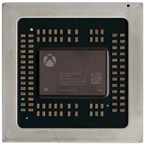 + + |
| manufacturer | TSMC + |
| market segment | Console + |
| max cpu count | 1 + |
| max memory | 24,576 MiB (25,165,824 KiB, 25,769,803,776 B, 24 GiB, 0.0234 TiB) + |
| max memory bandwidth | 304 GiB/s (311,296 MiB/s, 326.418 GB/s, 326,417.514 MB/s, 0.297 TiB/s, 0.326 TB/s) + |
| max memory channels | 12 + |
| microarchitecture | Enhanced Jaguar + and Polaris + |
| model number | Scorpio Engine + |
| name | Scorpio Engine + |
| package | BGA-2409 + |
| package contacts | 2,409 + |
| package length | 50 mm (5 cm, 1.969 in) + |
| package pitch | 0.8 mm (0.0315 in) + |
| package type | FC-OBGA + |
| package width | 50 mm (5 cm, 1.969 in) + |
| process | 16 nm (0.016 μm, 1.6e-5 mm) + |
| smp max ways | 1 + |
| supported memory type | GDDR5-6800 + |
| technology | CMOS + |
| thread count | 8 + |
| transistor count | 7,000,000,000 + |
| used by | Xbox One X + |
| word size | 64 bit (8 octets, 16 nibbles) + |
