From WikiChip
Xeon W-3225 - Intel
| Edit Values | |
| Xeon W-3225 | |
 | |
| General Info | |
| Designer | Intel |
| Manufacturer | Intel |
| Model Number | W-3225 |
| Part Number | CD8069504152705 |
| S-Spec | SRFFB |
| Market | Workstation |
| Introduction | June 3, 2019 (announced) June 3, 2019 (launched) |
| Release Price | $1,199.00 (tray) |
| Shop | Amazon |
| General Specs | |
| Family | Xeon W |
| Series | W-3200 |
| Locked | Yes |
| Frequency | 3,700 MHz |
| Turbo Frequency | 4,300 MHz (1 core) |
| Bus type | DMI 3.0 |
| Bus rate | 4 × 8 GT/s |
| Clock multiplier | 37 |
| Microarchitecture | |
| ISA | x86-64 (x86) |
| Microarchitecture | Cascade Lake |
| Core Name | Cascade Lake SP |
| Core Stepping | B1 |
| Process | 14 nm |
| Technology | CMOS |
| Word Size | 64 bit |
| Cores | 8 |
| Threads | 16 |
| Max Memory | 1 TiB |
| Multiprocessing | |
| Max SMP | 1-Way (Uniprocessor) |
| Electrical | |
| TDP | 160 W |
| Packaging | |
| Package | FCLGA-3647 (FCLGA) |
| Dimension | 76.16 mm × 56.6 mm |
| Pitch | 0.8585 mm × 0.9906 mm |
| Contacts | 3647 |
| Socket | Socket P, LGA-3647 |
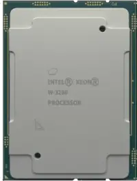
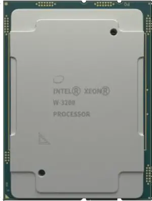
W-3225 is a 64-bit octa-core x86 enterprise performance workstation microprocessor introduced by Intel in 2019. This processor is fabricated on an enhanced 14nm++ process based on the Cascade Lake microarchitecture. The W-3225 operates at 3.7 GHz with a TDP of 160 W, a turbo boost frequency of up to 4.3 GHz and a turbo boost max of 4.4 GHz. This chip supports up to 1 TiB of hexa-channel DDR4-2666 memory.
Cache[edit]
- Main article: Cascade Lake § Cache
This processor has a non-default level 3 cache of 16.5 MiB, an amount usually found in the 12 cores part.
|
Cache Organization
Cache is a hardware component containing a relatively small and extremely fast memory designed to speed up the performance of a CPU by preparing ahead of time the data it needs to read from a relatively slower medium such as main memory. The organization and amount of cache can have a large impact on the performance, power consumption, die size, and consequently cost of the IC. Cache is specified by its size, number of sets, associativity, block size, sub-block size, and fetch and write-back policies. Note: All units are in kibibytes and mebibytes. |
|||||||||||||||||||||||||||||||||||||
|
|||||||||||||||||||||||||||||||||||||
Memory controller[edit]
|
Integrated Memory Controller
|
||||||||||||||
|
||||||||||||||
Expansions[edit]
Expansion Options |
|||||
|
|||||
Features[edit]
[Edit/Modify Supported Features]
Documents[edit]
Facts about "Xeon W-3225 - Intel"
| Has subobject "Has subobject" is a predefined property representing a container construct and is provided by Semantic MediaWiki. | Xeon W-3225 - Intel#pcie + |
| base frequency | 3,700 MHz (3.7 GHz, 3,700,000 kHz) + |
| bus links | 4 + |
| bus rate | 8,000 MT/s (8 GT/s, 8,000,000 kT/s) + |
| bus type | DMI 3.0 + |
| clock multiplier | 37 + |
| core count | 8 + |
| core name | Cascade Lake SP + |
| core stepping | B1 + |
| designer | Intel + |
| family | Xeon W + |
| first announced | June 3, 2019 + |
| first launched | June 3, 2019 + |
| full page name | intel/xeon w/w-3225 + |
| has advanced vector extensions | true + |
| has advanced vector extensions 2 | true + |
| has advanced vector extensions 512 | true + |
| has ecc memory support | true + |
| has extended page tables support | true + |
| has feature | Advanced Vector Extensions +, Advanced Vector Extensions 2 +, Advanced Vector Extensions 512 +, Advanced Encryption Standard Instruction Set Extension +, Hyper-Threading Technology +, Turbo Boost Technology 2.0 +, Turbo Boost Max Technology 3.0 +, Enhanced SpeedStep Technology +, Speed Shift Technology +, Trusted Execution Technology +, Intel vPro Technology +, Intel VT-x +, Intel VT-d +, Extended Page Tables +, Transactional Synchronization Extensions +, Memory Protection Extensions +, Secure Key Technology +, OS Guard +, Deep Learning Boost + and Identity Protection Technology + |
| has intel deep learning boost | true + |
| has intel enhanced speedstep technology | true + |
| has intel identity protection technology support | true + |
| has intel secure key technology | true + |
| has intel speed shift technology | true + |
| has intel supervisor mode execution protection | true + |
| has intel trusted execution technology | true + |
| has intel turbo boost max technology 3 0 | true + |
| has intel turbo boost technology 2 0 | true + |
| has intel vpro technology | true + |
| has intel vt-d technology | true + |
| has intel vt-x technology | true + |
| has locked clock multiplier | true + |
| has second level address translation support | true + |
| has simultaneous multithreading | true + |
| has transactional synchronization extensions | true + |
| has x86 advanced encryption standard instruction set extension | true + |
| instance of | microprocessor + |
| intel turbo boost max technology 3 0 frequency | 4,400 MHz (4.4 GHz, 4,400,000 kHz) + |
| isa | x86-64 + |
| isa family | x86 + |
| l1$ size | 512 KiB (524,288 B, 0.5 MiB) + |
| l1d$ description | 8-way set associative + |
| l1d$ size | 256 KiB (262,144 B, 0.25 MiB) + |
| l1i$ description | 8-way set associative + |
| l1i$ size | 256 KiB (262,144 B, 0.25 MiB) + |
| l2$ description | 16-way set associative + |
| l2$ size | 8 MiB (8,192 KiB, 8,388,608 B, 0.00781 GiB) + |
| l3$ description | 11-way set associative + |
| l3$ size | 16.5 MiB (16,896 KiB, 17,301,504 B, 0.0161 GiB) + |
| ldate | June 3, 2019 + |
| main image |  + + |
| manufacturer | Intel + |
| market segment | Workstation + |
| max cpu count | 1 + |
| max memory | 1,048,576 MiB (1,073,741,824 KiB, 1,099,511,627,776 B, 1,024 GiB, 1 TiB) + |
| max memory bandwidth | 119.21 GiB/s (122,071.04 MiB/s, 128.001 GB/s, 128,000.763 MB/s, 0.116 TiB/s, 0.128 TB/s) + |
| max memory channels | 6 + |
| microarchitecture | Cascade Lake + |
| model number | W-3225 + |
| name | Xeon W-3225 + |
| number of avx-512 execution units | 2 + |
| package | FCLGA-3647 + |
| part number | CD8069504152705 + |
| process | 14 nm (0.014 μm, 1.4e-5 mm) + |
| release price | $ 1,199.00 (€ 1,079.10, £ 971.19, ¥ 123,892.67) + |
| release price (tray) | $ 1,199.00 (€ 1,079.10, £ 971.19, ¥ 123,892.67) + |
| s-spec | SRFFB + |
| series | W-3200 + |
| smp max ways | 1 + |
| socket | Socket P + and LGA-3647 + |
| supported memory type | DDR4-2666 + |
| tdp | 160 W (160,000 mW, 0.215 hp, 0.16 kW) + |
| technology | CMOS + |
| thread count | 16 + |
| turbo frequency (1 core) | 4,300 MHz (4.3 GHz, 4,300,000 kHz) + |
| word size | 64 bit (8 octets, 16 nibbles) + |
| x86/has memory protection extensions | true + |