| Edit Values | |
| StrongARM µarch | |
| General Info | |
| Arch Type | CPU |
| Designer | DEC, ARM Holdings |
| Manufacturer | DEC, Intel |
| Introduction | February 5, 1996 |
| Process | 0.35 µm |
| Core Configs | 1 |
| Pipeline | |
| OoOE | No |
| Speculative | Yes |
| Reg Renaming | No |
| Stages | 5 |
| Decode | 1-way |
| Instructions | |
| ISA | ARMv4 |
| Cache | |
| L1I Cache | 16 KiB/core 32-way set associative |
| L1D Cache | 16 KiB/core 32-way set associative |
| Succession | |
StrongARM (SA) was a microarchitecture for DEC's series of ARM-based microprocessors branded under the same name. This microarchitecture was the result of a collaborative effort by DEC and ARM.
Contents
History[edit]
The StrongARM microarchitecture started as a collaborative project between ARM and DEC in the mid-1990s. This was one of two major microarchitectures developed by DEC around the same time (Alpha 21264 being the second one). The primary design goal was to develop a new class of high-performance low-power ARM-based processors. Earlier ARM architectures were simply insufficiently weak to power more advanced mobile devices such as PDAs and set-tops. Because of the new design goals, StrongARM implemented a number of new techniques not found in previous ARM architectures.
The historical significance of the StrongARM development cannot be overstated. StrongARM implemented the same ARM architecture as the ARM8 - ARMv4. The route ARM took to improve the ARM7 through the ARM8 was to widen the pipeline which allowed for double the speed at the cost of more die space for an identical process. ARM8 was consequently seldom licensed and has largely faded into obscurity. The StrongARM on the other hand, which was design using DEC's own in-house tools and semiconductor process, resulted in performance increase of up to 5 times as much. StrongARM enjoyed a series of design wins such as Psion 7 Series, Apple's MessagePad 2000/2100, Yakumo Alpha PDA, and various PDAs from HP's Jornada line. After being sold to Intel in 1997, the architecture was enhanced and went on to dominate the PDA and light mobile market for close to a decade before being sold to Marvell just prior to the smartphone boom in 2006.
It should be noted that in order to develop StrongARM, DEC had to license the ability to do so from ARM. This was the first time ARM gave a company an architecture license allowing them to actually design their own microarchitecture that implements the ARM instruction set. Previously ARM had only offered core licenses which gave a licensee an ARM-designed core they can use but they were not allowed to develop their own design.
It's also interesting to note that DEC was not doing well financially by 1997 with their Hudson fab being considerably underused (with some estimates putting it at only 40% utilization or less). The uncertainty put into question DEC's StrongARM manufacturing abilities which prevented some companies from switching to StrongARM. In early 1997 DEC filed a surprised patent infringement lawsuit against Intel over Alpha-related patents. Intel consequently countersued claiming DEC violated Intel's property rights. A settlement was eventually reached out of court with both companies signing a 10-year cross-licensing agreement and in an ironic twist of fate as part of a settlement, Intel agreed to buy DEC's semiconductor manufacturing operations for $700 million which included the Hudson, Mass foundry as well as DEC's development operations in Jerusalem, Israel and Austin, Texas.
Process Technology[edit]
- See also: 0.35 µm process
StrongARM was manufactured on a 0.35 µm process at DEC's own Hudson foundry. The process had a 0.35 µm drawn gate length and 0.25 µm effective channel length. The CMOS process had 3 metal layers and allowed for a supply voltage of 1.5 V with up to 2 V for highest clocks.
Architecture[edit]
| This section is empty; you can help add the missing info by editing this page. |
Memory Hierarchy[edit]
- Cache
- L1 Instruction Cache
- 16 KiB, 32-way set associative
- L1 Data Cache
- 16 KiB, 32-way set associative
- Write-back policy
- No L2 cache
- L1 Instruction Cache
- TLB
- ITLB
- 32-entry, fully associative
- Each entry can map 4 KiB, 64 KiB, and 1 MiB pages
- DTLB
- 32-entry, fully associative
- Each entry can map 4 KiB, 64 KiB, and 1 MiB pages
- ITLB
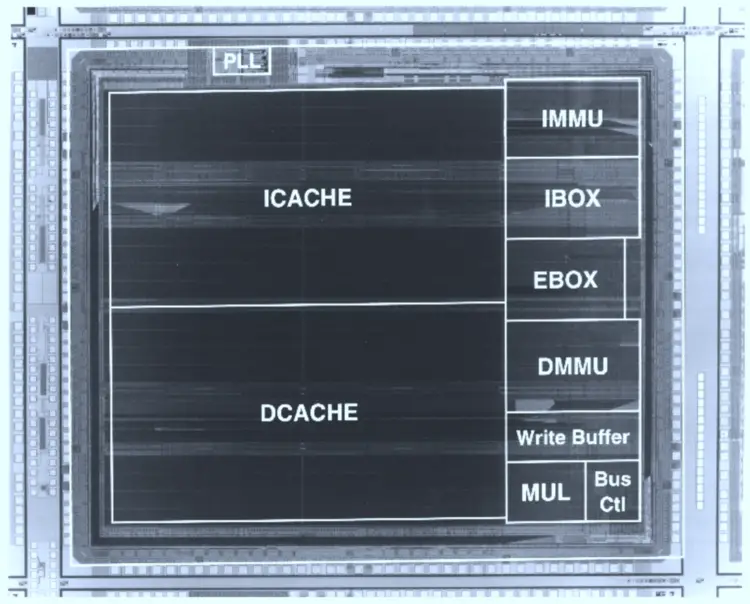
Die[edit]
- 2,100,000 transistors
- 0.35 µm using 3 metal layers
- 7.8 mm x 6.4 mm
- 49.92 mm² die size
- TQFP-144 package
All StrongARM chips[edit]
| This section is empty; you can help add the missing info by editing this page. |
References[edit]
- Witek, Rich, and James Montanaro. "StrongARM: a high-performance ARM processor." Compcon'96. 'Technologies for the Information Superhighway' Digest of Papers. IEEE, 1996.
- Dobberpuhl, Daniel W. "Circuits and technology for Digital's StrongARM and ALPHA microprocessors [CMOS technology]." Advanced Research in VLSI, 1997. Proceedings., Seventeenth Conference on. IEEE, 1997.
| codename | StrongARM + |
| core count | 1 + |
| designer | DEC + and ARM Holdings + |
| first launched | February 5, 1996 + |
| full page name | dec/microarchitectures/strongarm + |
| instance of | microarchitecture + |
| instruction set architecture | ARMv4 + |
| manufacturer | DEC + and Intel + |
| microarchitecture type | CPU + |
| name | StrongARM + |
| pipeline stages | 5 + |
| process | 350 nm (0.35 μm, 3.5e-4 mm) + |
