| Interconnect Architectures | |
 | |
| Concepts | |
| General | |
| Peripheral | |
| Storage Devices | |
| Audio Devices | |
NVLink is a proprietary system interconnect architecture that facilitates coherent data and control transmission accross multiple Nvidia GPUs and supporting CPUs.
Overview
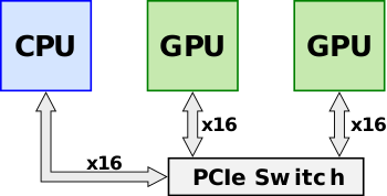
Announced in early 2014, NVLink was designed as an alternative solution to PCI Express with higher bandwidth and additional features (e.g., shared memory) specifically designed to be compatible with Nvidia's own GPU ISA for multi-GPU systems. Prior to the introduction of NVLink with Pascal (e.g., Kepler), multiple Nvidia's GPUs would sit on a shared PCIe bus. Although direct GPU-GPU transfers and accesses were already possible using Nvidia's Unified Virtual Addressing over the PCIe bus, as the size of data sets continued to grow, the bus became a growing system bottleneck. Throughput could further improve through the use of a PCIe switch.
NVLink is designed to replace the inter-GPU-GPU communication from going over the PCIe lanes. It's worth noting that NVLink was also designed for CPU-GPU communication with higher bandwidth than PCIe. Although it's unlikely that NVLink would be implemented on an x86 system by either AMD or Intel, IBM has collaborate with Nvidia to support NVLink on their POWER microprocessors. For support microprocessors, the NVLink can eliminate PCIe entirely for all links.
NVLink 1.0
NVLink 1.0 was first introduced with the GP100 GPGPU based on the Pascal microarchitecture. IBM also added support it with POWER8+.
NVLink 2.0
NVLink 2.0 was first introduced with the V100 GPGPU based on the Volta microarchitecture along with IBM's POWER9.

