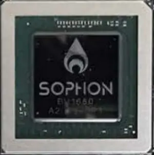
Template:mpu Sophon BM1680 is a neural processor designed by Bitmain and introduced in 2017. The BM1680 is capable of performing both network inference and network training. Capable of delivering up to 2 TFLOPS (SP), the BM1680 has a typical power dissipation of 25 W with a peak power of 41 W. The chip was taped-out in April 2017 and began sampling in June.
Manufactured on TSMC's 28HPC+ process, the BM1680 is capable of 80 billion algorithmic operations per second. Bitmain claims the chip is designed not only for inference, but also for training of neural networks, suitable for working with the common ANNs such as CNN, RNN, and DNN.
Overview
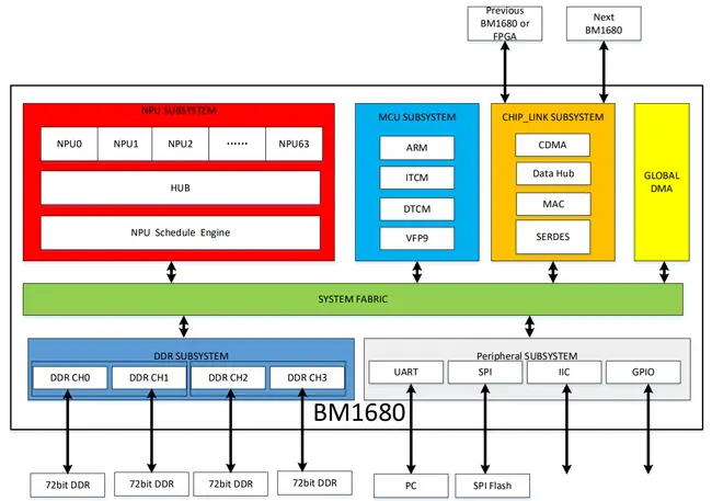
The chip consists of five subsystems: NPU, MCU, Chip Link, Memory, and Peripherals.
The MCU Subsystem is a low-power 32-bit embedded ARM microcontroller which can be boot from SPI Flash (ITCM interface). The microcontroller has an 8 KiB of L1I$ and 8 KiB of L1D$. Additionally, there is also a VPFv2 coprocessor for floating point operations support.
The NPU Subsystem consists of 64 NPUs, the hub, and an NPU Schedule Engine. The scheduling engine is in charge of controlling the data flow to the individual NPUs. Bitmain has not many intimate details of the NPU cores but each core is known to have 512 KiB of program-visible SRAM and supports 64 single-precision operations. With a total of 64 NPUs, the chip has a total of 32 MiB of cache and a peak performance of 2 TFLOPS (single-precision).
BMDNN Chiplink
The chip incorporates Bitmain's proprietary fabric called BMDNN Chiplink technology. The fabric is a flexible, low latency link that communicates over a high-speed SerDes PHY. Two ports are available on each chip which allows multiple BM1680s to be daisy chained together to form a larger network.
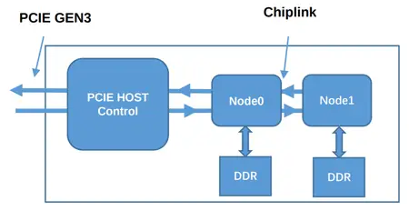
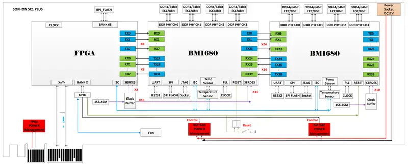
In a typical configuration (i.e., a PCIe accelerator card), two BM1680s chips are wired together using chiplink. The first node in the chain is then connected to a host control (e.g., a custom ASIC unit or simply an FPGA) which provides a PCIe interface to the host processor (e.g., on a typical server a Xeon). Data from the host processor is then sent to the host controller on the accelerator unit which is then distributed across all the NPUs on all the available nodes.
Current offering by Bitmain is limited to two BM1680s chips per accelerator card, however in theory the chip can be chained to form a much larger network. The primary limitations of the network are power consumption and thermal dissipation as well as PCIe bandwidth which Bitmain requires to be x4 lanes per node (or 3.9 GB/s, 8 GT/s). For example, current offerings by Bitmain features two nodes on a PCIe Gen3 x8 card.
Below is a schematic of Bitmain's SC+ PCIe Gen 3 accelerator card.
Memory controller
|
Integrated Memory Controller
|
||||||||||||||
|
||||||||||||||
Expansions
- SPI Flash Controller
- UART
- Two-wire I2C
| Has subobject "Has subobject" is a predefined property representing a container construct and is provided by Semantic MediaWiki. | Sophon BM1680 - Bitmain#package + |
| core voltage | 0.9 V (9 dV, 90 cV, 900 mV) + |
| core voltage tolerance | 5% + |
| designer | Bitmain + |
| family | Sophon + |
| first announced | October 25, 2017 + |
| first launched | November 8, 2017 + |
| full page name | bitmain/sophon/bm1680 + |
| has ecc memory support | true + |
| instance of | microprocessor + |
| io voltage | 1.8 V (18 dV, 180 cV, 1,800 mV) + |
| io voltage tolerance | 5% + |
| ldate | November 8, 2017 + |
| main image |  + + |
| manufacturer | TSMC + |
| market segment | Artificial Intelligence + |
| max memory | 16,384 MiB (16,777,216 KiB, 17,179,869,184 B, 16 GiB, 0.0156 TiB) + |
| max memory bandwidth | 79.47 GiB/s (81,377.28 MiB/s, 85.33 GB/s, 85,330.263 MB/s, 0.0776 TiB/s, 0.0853 TB/s) + |
| max memory channels | 4 + |
| max operating temperature | 125 °C + |
| min operating temperature | 0 °C + |
| model number | BM1680 + |
| name | Sophon BM1680 + |
| package | FCBGA-1599 + |
| peak flops (single-precision) | 2,000,000,000,000 FLOPS (2,000,000,000 KFLOPS, 2,000,000 MFLOPS, 2,000 GFLOPS, 2 TFLOPS, 0.002 PFLOPS, 2.0e-6 EFLOPS, 2.0e-9 ZFLOPS) + |
| process | 28 nm (0.028 μm, 2.8e-5 mm) + |
| supported memory type | DDR4-2666 + |
| tdp | 41 W (41,000 mW, 0.055 hp, 0.041 kW) + |
| tdp (typical) | 25 W (25,000 mW, 0.0335 hp, 0.025 kW) + |
| technology | CMOS + |


