From WikiChip
ARM250 - Microarchitectures - ARM
| Edit Values | |
| ARM250 µarch | |
| General Info | |
| Arch Type | CPU |
| Designer | ARM Holdings |
| Manufacturer | VLSI Technology |
| Introduction | 1992 |
| Process | 1 µm |
| Core Configs | 1 |
| Pipeline | |
| Type | Scalar, Pipelined |
| Stages | 3 |
| Decode | 1-way |
| Instructions | |
| ISA | ARMv2a |
| Cores | |
| Core Names | ARM250 |
| Succession | |
ARM250 was a system on a chip microarchitecture that was introduced by ARM Holdings around the same time the ARM6 was introduced.
Contents
History
- See also: ARM's History
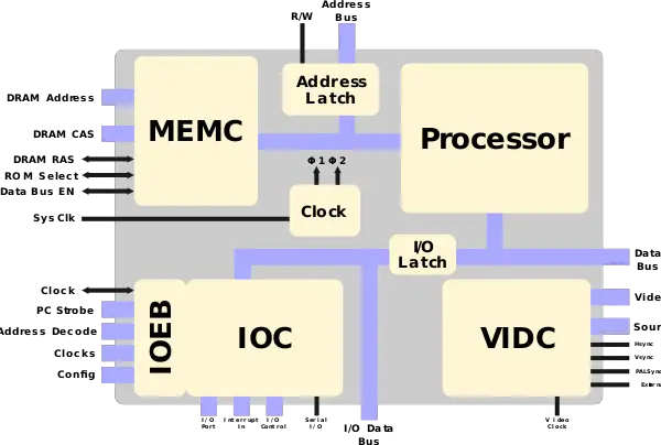
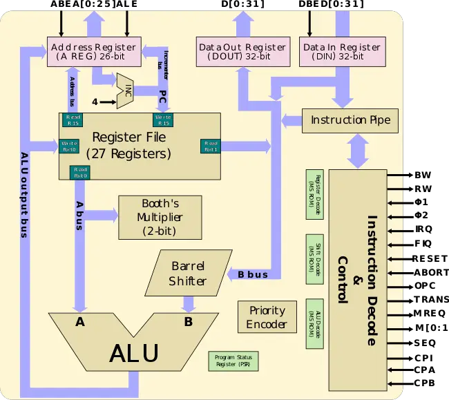
With the development of the ARM6 and a process shrink by VTI, ARM took the opportunity to introduce the ARM250. The ARM250 is a very high integration chip - incorporating the ARM3 core along with most of the new MMU logic that was developed for the ARM6 along with all the support chips that were previously needed for the ARM3/2 - the MEMC chip (Memory Controller), VIDC chip (Video Controller), IOC/IOEB (I/O Controller).
Note that the added L1 cache found on the ARM3 is not found on the ARM250.
Process Technology
- See also: 1 µm process
The ARM250 was implemented on a 1 µm double-level metal (DLM) CMOS process.
Architecture
Block Diagram
Entire Chip
Core
Die
- 1-micron process CMOS
- 2 metal layers
- 58 mm² die size
- 98,019 transistors
- $25 (for 100K quantities)
References
- Muller, Mike. "ARM6: a high performance low power consumption macrocell." Compcon Spring'93, Digest of Papers.. IEEE, 1993.
Documents
- ARM250 Datasheet, August 11, 1992
Facts about "ARM250 - Microarchitectures - ARM"
| codename | ARM250 + |
| core count | 1 + |
| designer | ARM Holdings + |
| first launched | 1992 + |
| full page name | arm holdings/microarchitectures/arm250 + |
| instance of | microarchitecture + |
| instruction set architecture | ARMv2a + |
| manufacturer | VLSI Technology + |
| microarchitecture type | CPU + |
| name | ARM250 + |
| pipeline stages | 3 + |
| process | 1,000 nm (1 μm, 0.001 mm) + |

