'File:Spiffy Pictures.EXE Buttons Z By Anti Rex 3000.png

| Edit Values | |
| Cortex-A510 µarch | |
| General Info | |
| Arch Type | CPU |
| Designer | ARM Holdings |
| Manufacturer | TSMC, Samsung, GlobalFoundries, SMIC |
| Introduction | May 25, 2021 |
| Process | 7 nm, 6 nm, 5 nm |
| Core Configs | 1, 2 |
| Pipeline | |
| Type | In-order |
| OoOE | No |
| Speculative | Yes |
| Reg Renaming | No |
| Decode | 3-way |
| Instructions | |
| ISA | ARMv9.0 |
| Extensions | FPU, NEON, SVE, SVE2, TrustZone |
| Cache | |
| L1I Cache | 32-64 KiB/core 4-way set associative |
| L1D Cache | 32-64 KiB/core 4-way set associative |
| L2 Cache | 0-512 KiB/cluster 4-way set associative |
| Succession | |
Cortex-A510 (codename Klein) is an ultra-high efficiency microarchitecture designed by ARM Holdings as a successor to the Cortex-A55. The Cortex-A510, which implements the ARMv9.0 ISA, is typically found in smartphone and other embedded devices. Often A510 cores are combined with higher performance processors (e.g. based on Cortex-A710) in DynamIQ big.LITTLE configuration to achieve better energy/performance.
Note that this microarchitecture is designed as a synthesizable IP core and is sold to other semiconductor companies to be implemented in their own chips.
Contents
Process Technology
The Cortex-A510 was primarily designed to take advantage of TSMC's 7 nm, 6 nm, 5 nm as well as Samsung's 7 nm and 5 nm.
Architecture
The Cortex-A510 is a brand new ground-up CPU design. It borrows advanced processor components from Arm's high-performance cores - such as the branch prediction and prefetchers - to extract high performance from a traditional in-order core design. The Cortex-A512 is also designed to seamlessly integrate along with higher-performance cores through Arm's DynamIQ big.LITTLE technology.
Key changes from Cortex-A55
- Brand new ground-up design
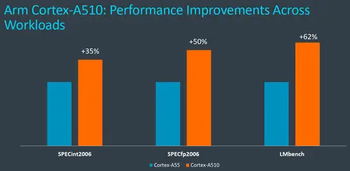
- Higher performance (Arm claims: +35% IPC (SPECint 2006) / +50% IPC (SPECfp 2006)
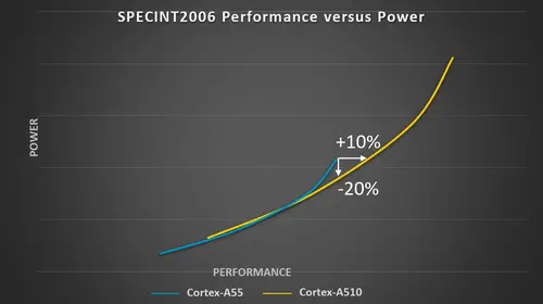
- Lower power (Arm claims: -20% energy @ iso-performance / +10% performance @ iso-power)
- Core Complex with a merged core architecture
- Two independent cores
- One shared vector unit
- Configurable 64b or 128b pipe
- Front-End
- Wider fetch (128b/cycle, up from 64b)
- Wider decoder (3-way, up from 2-way)
- New branch predictors
- New prefetchers
- Back-End
- In-order
- Memory Subsystem
- Larger L1 (32-64 KiB)
- Larger L2 (0-512 KiB, up from 0-256 KiB)
- 2x bandwidth L2->L3
- Wider loads (128b/cycle, up from 64b/cycle)
- 2x loads (2 lds/cycle, up from 1/cycle)
- New ISA Support
- ARMv9.0 ISA
- SVE, SVE2 support
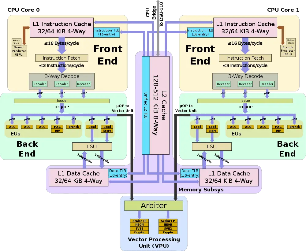
Block Diagram
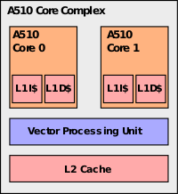
Core Complex
Memory Hierarchy
The Cortex-A510 has a private L1I, L1D, and cluster-wide L2 cache.
- Cache
- L1I Cache
- Private to core
- 32 KiB OR 64 KiB, 4-way set associative
- 64-byte cache lines
- Virtually-indexed, physically-tagged (VIPT) behaving as physically-indexed, physically-tagged (PIPT)
- Single Error Detect (SED) parity cache protection
- Pseudo-random cache replacement policy
- L1D Cache
- Private to core
- 32KB or 64KB, 4-way set associative
- Virtually-Indexed, Physically-Tagged (VIPT) behaving as Physically-Indexed, Physically-Tagged (PIPT)
- Error Correcting Code (ECC) cache protection
- 64-byte cache lines
- Pseudo-random cache replacement policy
- L2 Cache
- Private to complex
- 128 KiB OR 192 KiB OR 256 KiB OR 384 KiB OR 512 KiB, 8-way set associative
- 64-byte cache lines
- Can be configured as 1-2 slices
- Slice includes: data RAMs, L2 tags, L2 replacement RAM, and L1 duplicate tag RAMs
- Slice can be configured as single/dual partitions for up to two concurrent accesses to different L2 ways
- L1I Cache
The Cortex-A510 features an instruction TLB (ITLB) and data TLB (DTLB) which are private to each core and an L2 TLB that is private to the core complex.
- TLBs
- ITLB
- 16-entries
- fully associative
- TLB hits return the PA to the instruction cache
- DTLB
- 16-entries
- fully associative
- TLB hits return the PA to the data cache
- L2 TLB
- 8-way set associative
- Shared by both cores in the complex
- ITLB
Overview
The Cortex-A510 is Arm's successor to the Cortex-A55 which was introduced four years earlier. Designed to be ultra-low-power and versatile, this core can be used as a standalone CPU in low-power SoCs or serve the efficient core as part of a DynamIQ big.LITTLE architecture using the DSU-110. To maintain high efficiency, the Cortex-A510 remains an in-order architecture. However, by borrowing high-performance components such as state-of-the-art branch predictors and prefetchers, the Cortex-A510 enjoys significantly higher performance over its predecessor through higher effective instruction stream throughput. The Cortex-A55 is the first small core from Arm to feature the Armv9 ISA along with the Scalable Vector Extension (SVE) and SVE2 extensions.
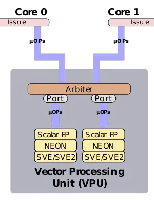
The Cortex-A510 introduces the concept of a Core Complex along with a merged core architecture. A core complex tightly integrates two Cortex-A510 cores, sharing a single common level 2 cache and vector processing unit (VPU). Like any other Arm IP, the Cortex-A510 complex can be instantiated within a standard DSU cluster as any other core would. The only difference is that you are dealing with two cores at once in a single instance. Because the effective utilization of the vector unit on the small cores is quite low, by implementing a single vector unit for two A510 cores, the silicon area is maintained relatively low while still offering good peak performance when needed.
Core
The Cortex-A510 is a new ground-up design. Compared to its predecessor, the Cortex-A55, the A510 is wider, but the underlying architecture remains an in-order pipeline. The choice to remain with an in-order pipeline design was driven by the overall simplicity of the design which maximizes power efficiency and area usage. Each Cortex-A510 core integrates its own private level 1 instruction cache and private level 1 data cache.
The Cortex-A510 features a 10-stage pipeline.
Front-end
The front-end of the Cortex-A510 fetches instructions from the private level 1 instruction cache and streams them to decode. The L1I$ on the A510 can be configured as 32 KiB or 64 KiB, both are 4-way set associative.
Fetch & Decode
The A510 speculatively fetches instructions streams. The A510 can predict conditional, unconditional, A32/T32 branch switches, and indirect procedure call/return branches. Each cycle, the A510 can fetch up to 128b (16B) from the instruction cache; twice the fetch bandwidth of the Cortex-A55. This allows it to deliver up to four instructions to decode.
Because the A510 is an in-order design, the performance of the core largely depends on the ability of the hardware to correctly predict future instruction stream patterns and paths. Advanced branch predictors along with aggressive prefetchers that were taken from Arm's big cores (i.e., Cortex-A710) were integrated into the A510 in order to allow for higher effective instruction stream bandwidth.
From the fetch stream, up to three instructions are sent to decode. The Cortex-A510 features a 3-wide decode, 50% wider than the Cortex-A55.
Back-end
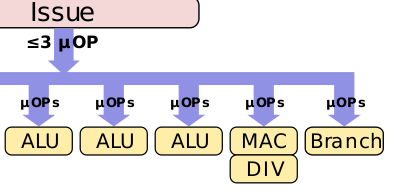
Each cycle, up to three instructions are decoded and sent to the back-end for execution. To match fetch and decode width, the A510 features a 3-wide issue and execute. The A510 is 50% wider than its predecessor, the Cortex-A55 which was 2-wide.
Each cycle, up to three μOPs may be sent to execution. The A510 features a 10-wide pipe. Compared to the Cortex-A55, Arm added a third ALU pipeline to increase integer workload bandwidth. With a 3-wide issue, the A510 can issue up to three ALU instructions to the three pipelines each cycle. There is a separate pipe for complex ALU operations as well as a separate ALU for performing branch operations.
Due to the nature of an in-order pipeline, Arm says a lot of work went into the forwarding capabilities of the design and the multi-issue capabilities of the execution engines. Special care was taken to maintain the execution bandwidth up in more cases while being less sensitive to specific instruction scheduling. Due to the inter-instruction dependencies nature of an in-order pipeline, poorly scheduled code can create backups and significantly reduce the effective execution throughput. Arm stated that in the Cortex-A510, a lot of attention has gone into maximizing this concern while keeping everything in order for maximum efficiency.
Memory subsystem
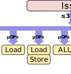
The Cortex-A510 has been significantly improved over the A55. Like the Cortex-A55, the Cortex-A510 maintains two memory pipelines. Whereas the A55 could perform one load on one pipe and one store on the other, the Cortex-A510 is capable of executing loads on both pipes. In other words, the A510 supports up to two loads per cycle or - alternatively - one load and one store per cycle. Arm also doubled the width of the data loads on the A510. Data loads are 128b-wide now, double the 64b-wide loads of the Cortex-A55. Because the A510 supports up to two loads per cycle or 2x128b loads, the peak L1 cache bandwidth is now 4x compared to the A55.
The Cortex-A510 features a private L1 data cache which can be configured with a capacity of 32 KiB or 64 KiB. Both configurations are organized as a 4-way set associative. The bandwidth from the other caches was also doubled – the L2 and L3 bandwidths are doubled that of the Cortex-A55.
Data prefetching on the A510 also received special attention. Arm stated that technologies that were originally developed for the Cortex-X2 were carried over to the Cortex-A510 design. There are multiple complementary data prefetching algorithms implemented on the Cortex-A510.
Core Complex
That Cortex-A510 is integrated as part of a Complex. Normally, each complex would incorporate two Cortex-A510 cores. Both cores share a complex-private L2 cache and a complex-private vector processing unit. The rationale for a complex is the ability for the A510 to fully support the Armv9.0 ISA including the Scalable Vector Extension (SVE) and SVE2. With a single shared vector processing unit, the A510 can support peak vector performance when needed while conserving silicon area due to lower utilization when compared to the big cores. While the two-core complex is the default and encouraged configuration, customers can opt to use it in a single-core complex, allowing for a dedicated VPU and L2 cache but at higher silicon area.
Vector Processing Unit (VPU)
A major component of the core complex is the vector processing unit (VPU) which is private to the complex and is shared by both Cortex-A510's. Because typical vector workloads will usually be assigned to the big cores, the VPU utilization on the small cores is expected to be relatively low. To maximize silicon area usage while providing sufficient vector performance, a single VPU instance is shared by both cores.
Once a μOP is issued to the VPU from one of the cores it is sent to the arbitration unit. Arbitration is completely hardware-based with execution sharing and utilization being entirely transparent to software. There is no user or OS-level software intervention for the arbitration of vector unit accesses between the cores. Furthermore, from a software perspective, each core appears to have dedicated access to the vector unit. Scheduling is very fine-grained between the cores to make sure there is minimal overhead caused by the sharing. There is no penalty for sharing or using the VPU. Arm says that they see very minimal performance overhead due to the sharing of the VPU. In their own internal testing, on the SPECfp 2006 benchmark, they see around a 1% performance degradation if both cores are executing FP/vector instructions at the same time as they compete to use the vector datapath.
All scalar and floating-point NEON and SVE2 instructions are executed through the vector datapath. There is support for optional crypto as well. This datapath itself is configurable. Possible configurations include having two 64b or two 128b data pipes - twice the peak bandwidth delta between the two configurations. A configuration of 2x128b data pipes will offer twice the peak compute of the Cortex-55. Depending on the configuration, designers have the flexibility in deciding between area and performance depending on their application and workload characterization. In the 2x128b configuration, the Cortex-A510 complex can achieve 16 FP16 FLOPS/clk. Note that regardless of the vector unit size or configuration, for SVE, there is a 128b vector register file.
Performance claims
At the peak operating point of the Cortex-A55, the Cortex-A510 is capable of reaching the same performance at 20% less energy. Alternatively, within the same power budget, the A510 achieves 10% higher performance. Compared to the Cortex-A55, Arm says that the Cortex-A510 has around 35% higher IPC on SPECint 2006. On the SPECfp 2006 benchmark, Arm claims to see an even higher performance improvement at around 50%.
 |
|
Die
Advanced implementation die floorplan.
All Cortex-A510 Processors
| List of Cortex-A510-based Processors | ||||||||
|---|---|---|---|---|---|---|---|---|
| Main processor | Integrated Graphics | |||||||
| Model | Family | Launched | Process | Arch | Cores | Frequency | GPU | Frequency |
| Count: 0 | ||||||||
Bibliography
- Arm Tech Day, 2021
- Arm. personal communication. 2021.
Documents
| codename | Cortex-A510 + |
| core count | 1 + and 2 + |
| designer | ARM Holdings + |
| first launched | May 25, 2021 + |
| full page name | arm holdings/microarchitectures/cortex-a510 + |
| instance of | microarchitecture + |
| instruction set architecture | ARMv9.0 + |
| manufacturer | TSMC +, Samsung +, GlobalFoundries + and SMIC + |
| microarchitecture type | CPU + |
| name | Cortex-A510 + |
| process | 7 nm (0.007 μm, 7.0e-6 mm) +, 6 nm (0.006 μm, 6.0e-6 mm) + and 5 nm (0.005 μm, 5.0e-6 mm) + |
