Semiconductor & Computer Engineering
From WikiChip
File list
This special page shows all uploaded files.
First page |
Previous page |
Next page |
Last page |
| Date | Name | Thumbnail | Size | Description | Versions |
|---|---|---|---|---|---|
| 08:39, 21 August 2017 | kaby lake r sa.png (file) |  |
1.49 MB | Intel's {{intel|Kaby Lake R|l=core}} {{intel|System Agent}}. Cropped from an Image by Intel. * Annotated Version: kaby_lake_r_sa_(annotated).png | 1 |
| 06:54, 21 August 2017 | intel 8th gen core logs.png (file) |  |
1.26 MB | Intel's based 8th Generation Core. Image by Intel. | 1 |
| 06:32, 21 August 2017 | kaby-lake-r-product-brief.pdf (file) |  |
1.2 MB | Intel's {{intel|Kaby Lake R|l=core}} Product Brief. | 1 |
| 06:09, 21 August 2017 | kaby lake r (back, angled).png (file) | .png) |
6.24 MB | correction | 2 |
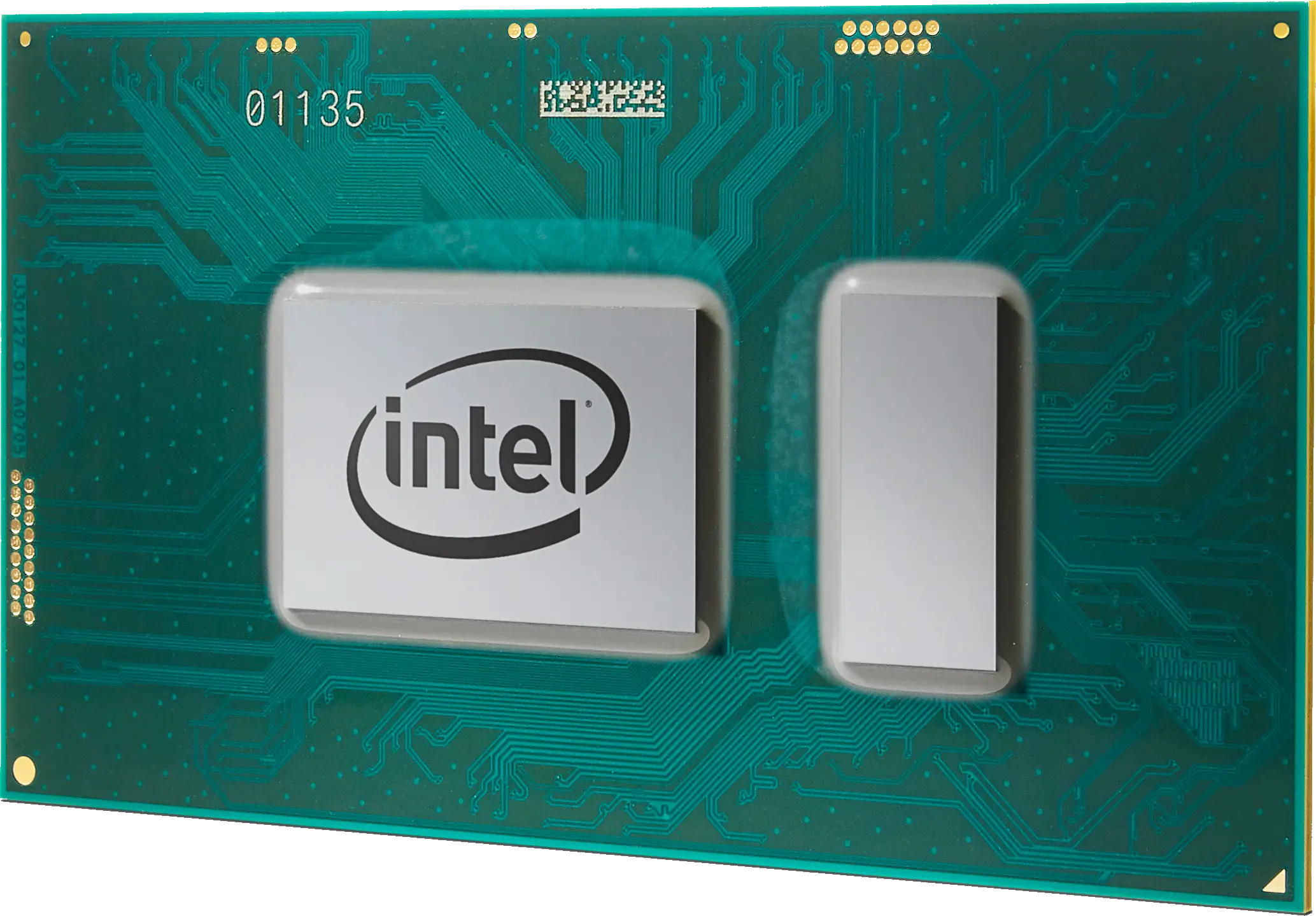
| 06:07, 21 August 2017 | kaby lake r (front, angled).png (file) | .png) |
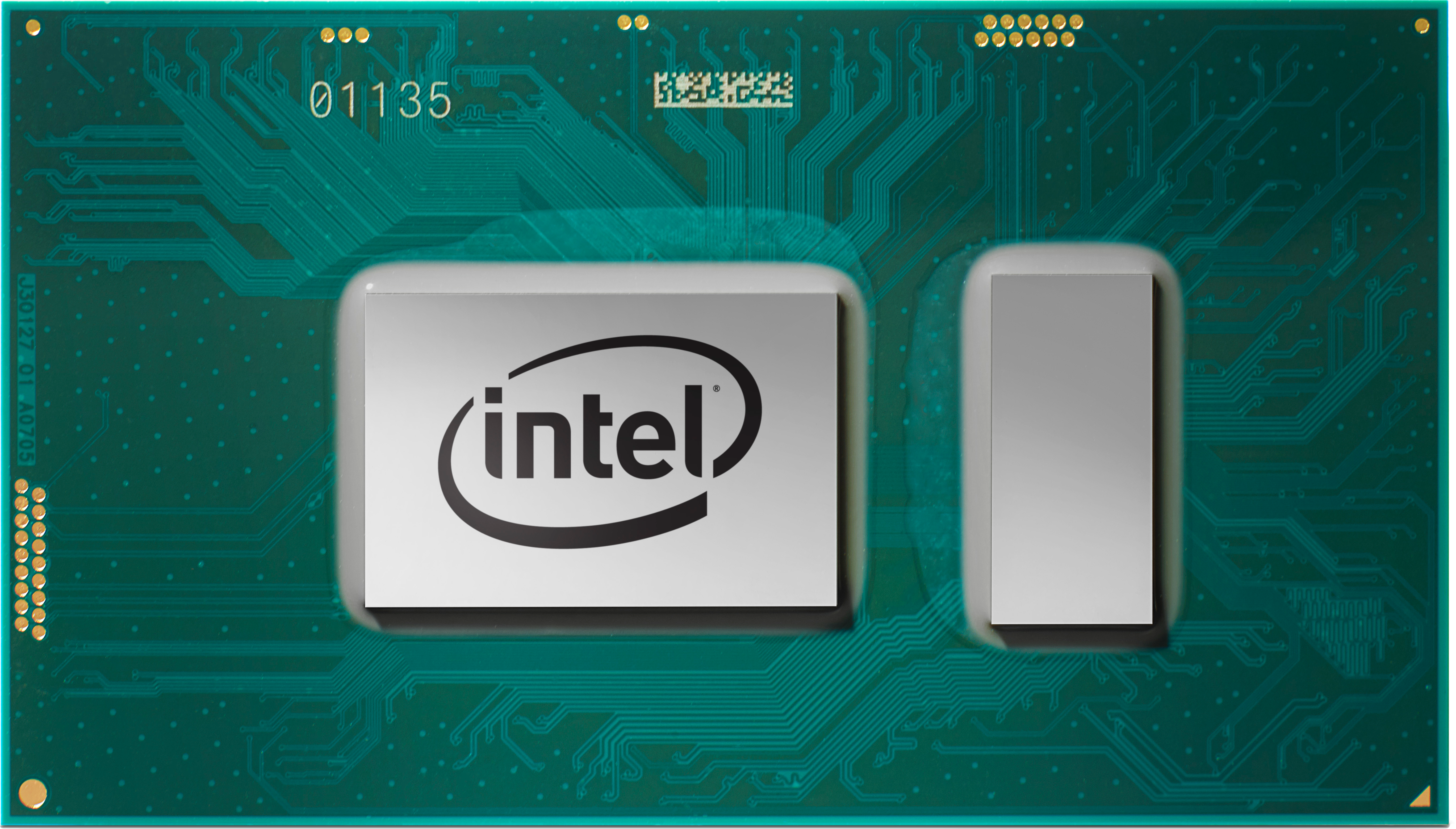
3.71 MB | Front of Intel {{intel|Kaby Lake R|l=core}}. Image by Intel. | 1 |
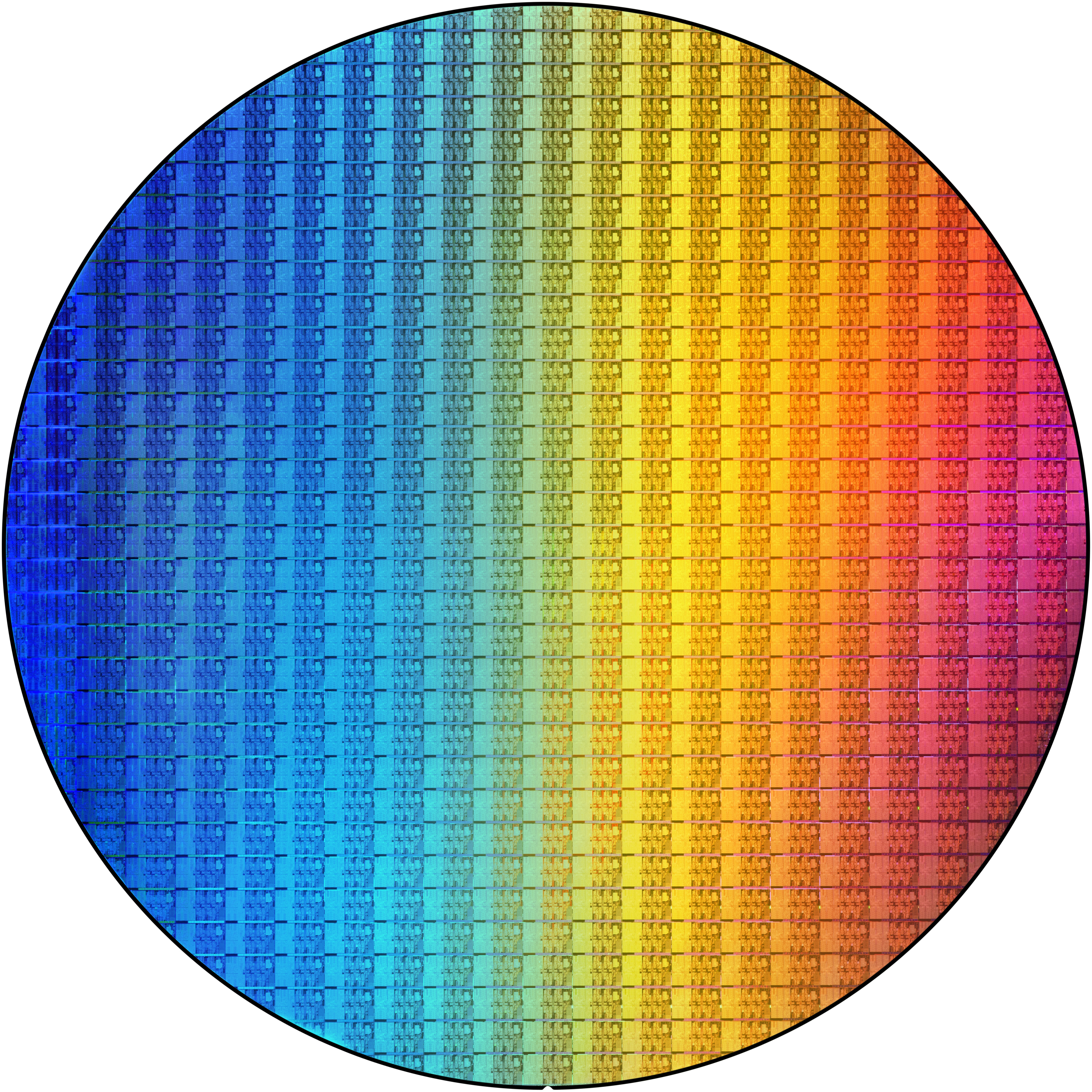
| 05:41, 21 August 2017 | intel kaby lake r wafer.png (file) |  |
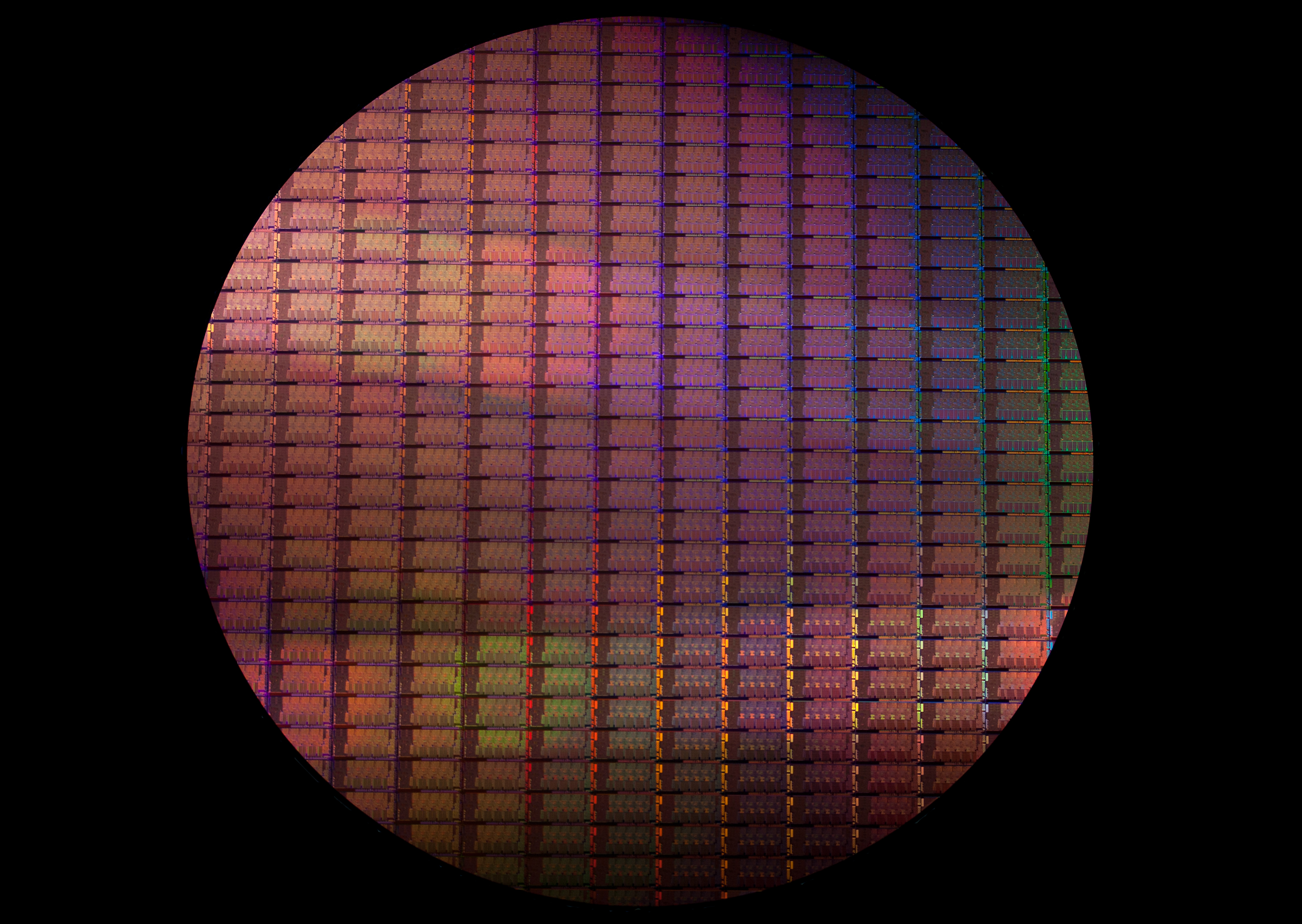
22.65 MB | Intel's {{intel|Kaby Lake R|l=core}} wafer. Image by Intel. | 1 |
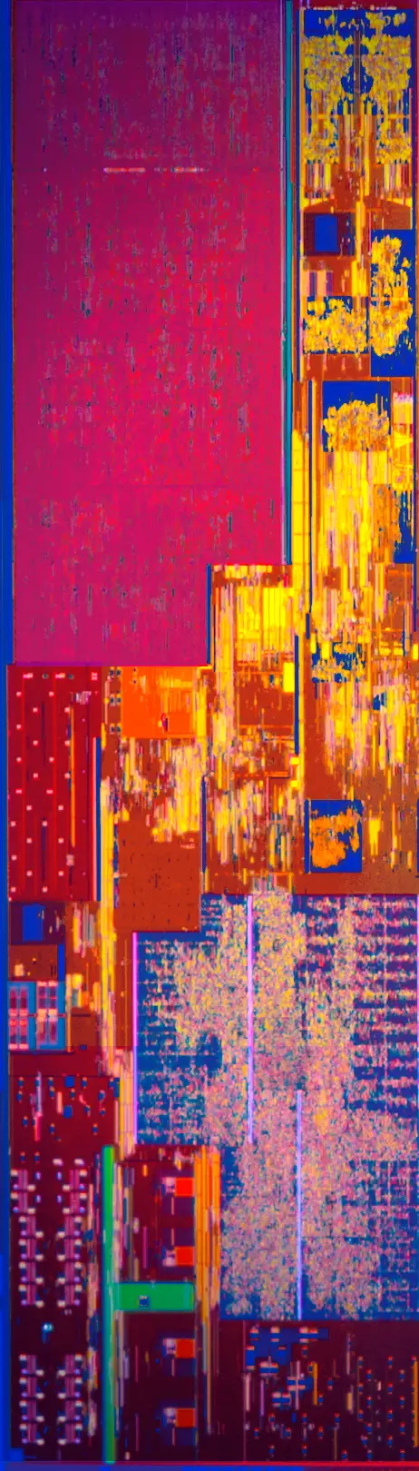
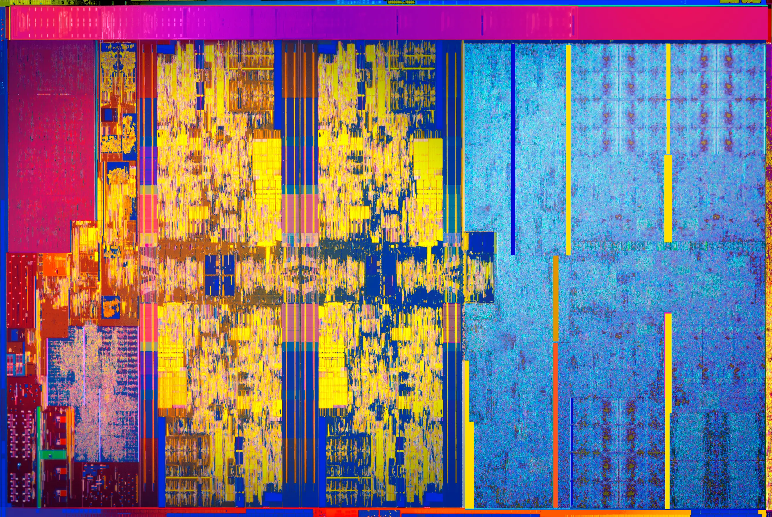
| 05:24, 21 August 2017 | kaby lake r die shot.png (file) |  |
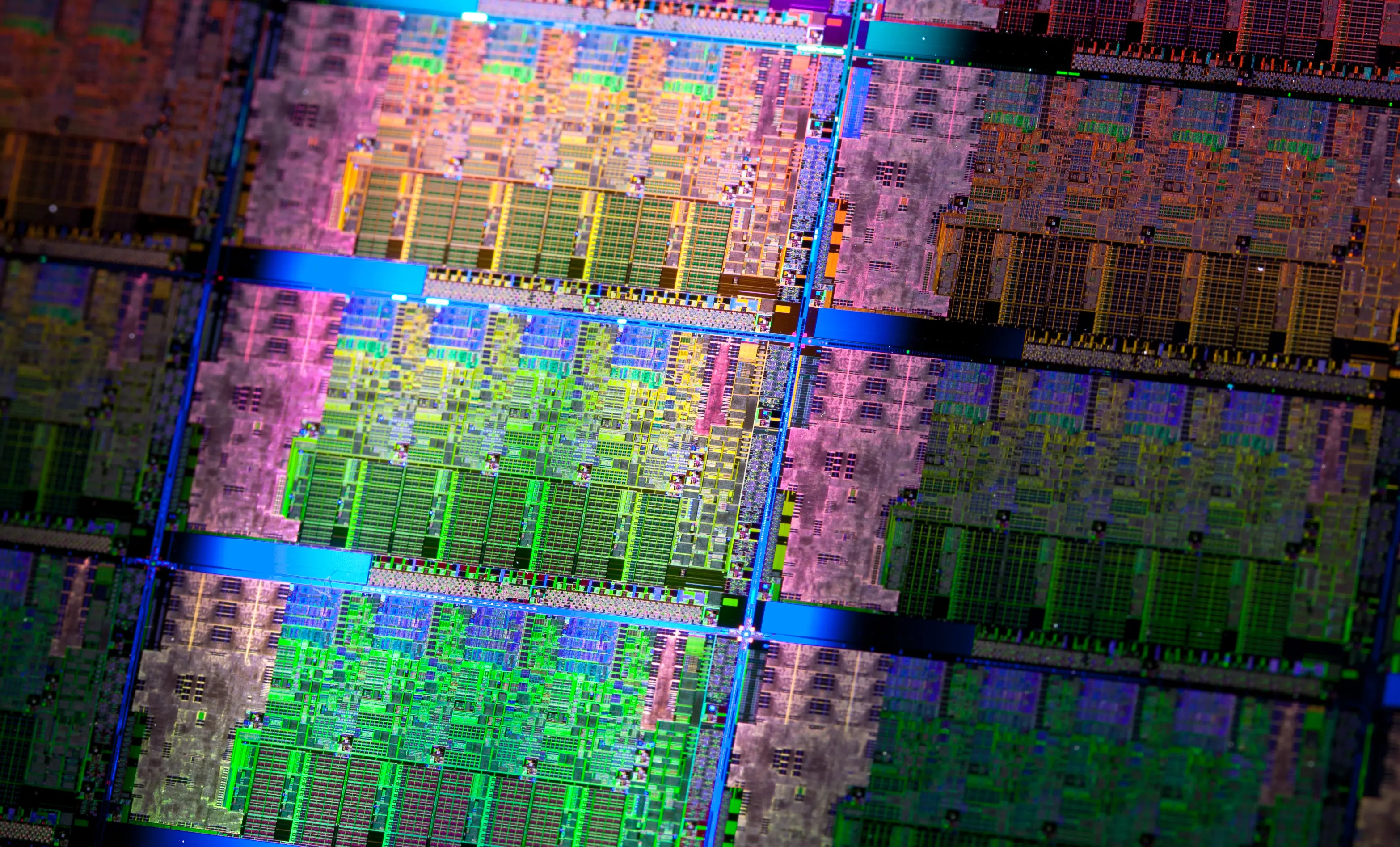
8.47 MB | Intel's {{intel|Kaby Lake R|l=core}} shit shot. Image by Intel. * Annotated Version: File:kaby_lake_r_die_shot_(annotated).png | 1 |
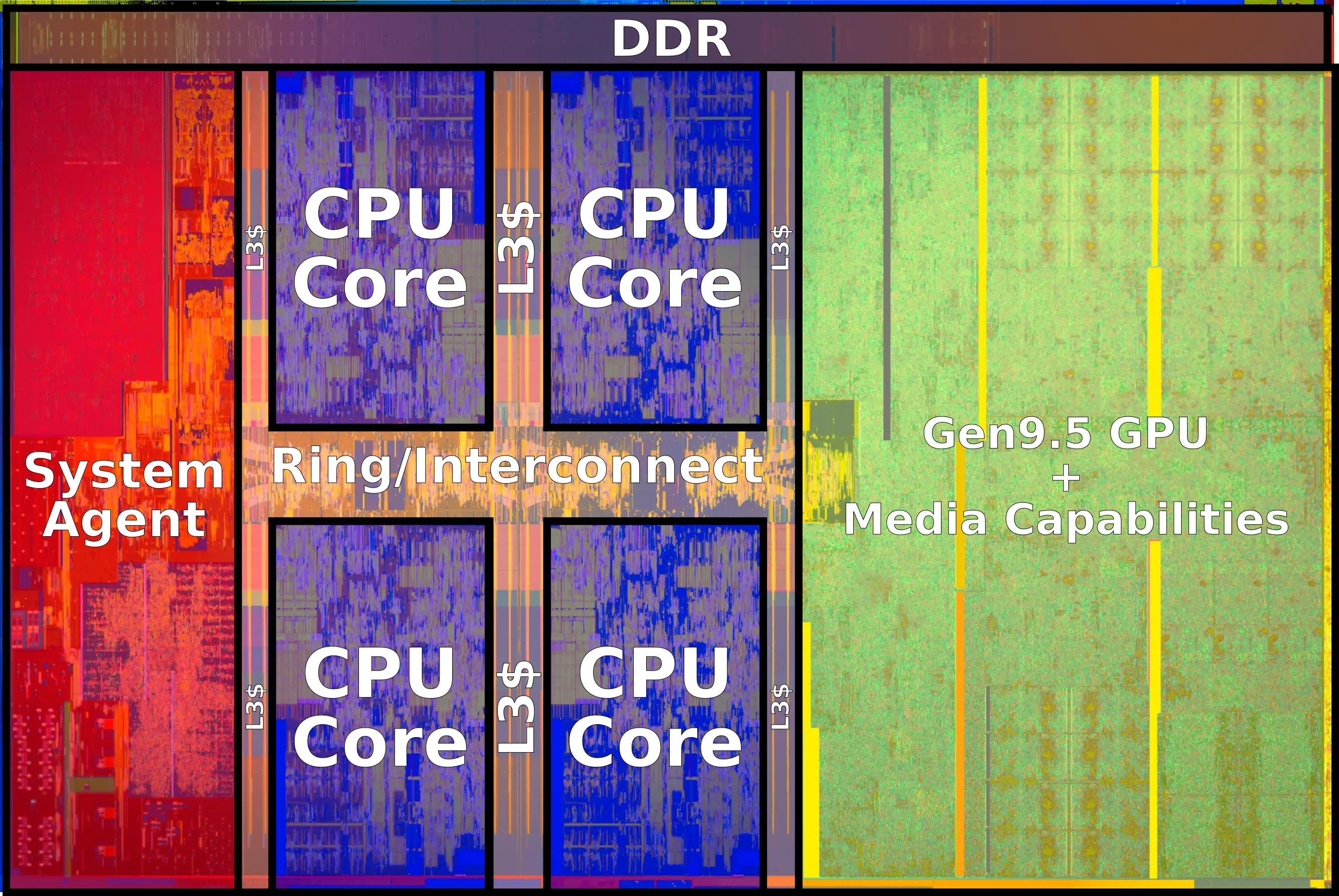
| 05:23, 21 August 2017 | kaby lake r die shot (annotated).png (file) | .png) |
7.15 MB | more general for main image | 2 |
| 05:12, 21 August 2017 | kaby lake r (front).png (file) | .png) |
15.3 MB | Front side of {{intel|Kaby Lake R|l=core}}. Image by Intel. | 1 |
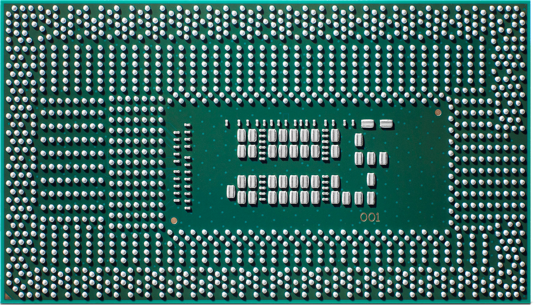
| 05:11, 21 August 2017 | kaby lake r (back).png (file) | .png) |
3.7 MB | Front side of {{intel|Kaby Lake R|l=core}}. Image by Intel. | 1 |
| 00:29, 13 August 2017 | after netburst frequency.png (file) |  |
350 KB | 1 | |
| 21:44, 12 August 2017 | Press45nm107 FINAL.pdf (file) |  |
564 KB | * Intel Demonstrates * High-k + Metal Gate Transistor Breakthrough on 45 nm Microprocessors | 1 |
| 21:43, 12 August 2017 | 45nmSummaryFoils.pdf (file) |  |
938 KB | * New Intel 45 nm Processors * Reinvented transistors and new products * November, 2007 | 1 |
| 21:43, 12 August 2017 | SandToCircuit FINAL.pdf (file) |  |
6.46 MB | From sand to circuits | 1 |
| 21:31, 12 August 2017 | Rattner IDFA Final.pdf (file) |  |
2.36 MB | * Justin Rattner * Senior Fellow * Chief Technology Officer | 1 |
| 21:30, 12 August 2017 | 20060308 Pawlowski.pdf (file) |  |
1.2 MB | Intel® {{intel|core|Core Microarchitecture|l=arch}} * Steve Pawlowski; Intel Senior Fellow; CTO, GM Architecture & Planning; Digital Enterprise Group * Ofri Wechsler; Intel Fellow; Director, CPU Architecture; Mobility Group | 1 |
| 21:21, 12 August 2017 | NGMA IDF Press Mar 8 PDF Set.pdf (file) |  |
6.6 MB | * Intel® {{intel|Core Microarchitecture|l=arch}} * March 8, 2006 * Bob Valentine, Architect, Intel Architecture Group | 1 |
| 21:21, 12 August 2017 | Multicore MATS002 999 pct.pdf (file) |  |
2.82 MB | * Intel {{intel|core|Multi-core Architecture and Implementations|l=arch}} * Intel Architecture Group * March 7, 2006 * Session: MATS002 | 1 |
| 21:17, 12 August 2017 | Intel(R) Core(TM)2 Extreme Processor Product Brief.pdf (file) |  |
218 KB | Product Brief: Intel® {{intel|Core 2 Extreme}} Processor | 1 |
| 21:17, 12 August 2017 | Intel(R) Core(TM)2 Duo Processor Product Brief.pdf (file) |  |
191 KB | Product Brief: Intel® {{intel|Core 2 Duo}} Desktop Processor | 1 |
| 20:58, 12 August 2017 | Inside Intel® Core Microarchitecture.pdf (file) |  |
714 KB | * White Paper: Inside Intel® Core TM Microarchitecture * Setting New Standards for * Energy-Efficient Performance | 1 |
| 18:06, 12 August 2017 | tejas cancelled.jpg (file) |  |
186 KB | Intell {{intel|Enhanced NetBurst|l=arch}} cancelled | 1 |
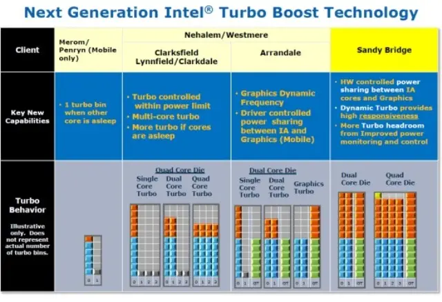
| 19:13, 6 August 2017 | sandy bridge new turbo.png (file) |  |
323 KB | Intel {{intel|Sandy Bridge|l=arch}} turbo improvements. Intel IDF, 2010. | 1 |
| 13:47, 30 July 2017 | sandy bridge wafer angled 2.png (file) |  |
17.65 MB | Image of an Intel {{intel|Sandy Bridge|l=arch}} wafer at an angle. Image by Intel. | 1 |
| 13:47, 30 July 2017 | sandy bridge wafer angled 3.png (file) |  |
15.04 MB | Image of an Intel {{intel|Sandy Bridge|l=arch}} wafer at an angle. Image by Intel. | 1 |
| 13:45, 30 July 2017 | sandy bridge wafer angled 1.png (file) |  |
9.85 MB | Image of an Intel {{intel|Sandy Bridge|l=arch}} wafer at an angle. Image by Intel. | 1 |
| 13:26, 30 July 2017 | sandy bridge die on a wafer.png (file) |  |
15.87 MB | Intel {{intel|Sandy Bridge|l=arch}} die on a wafer. Image by Intel. | 1 |
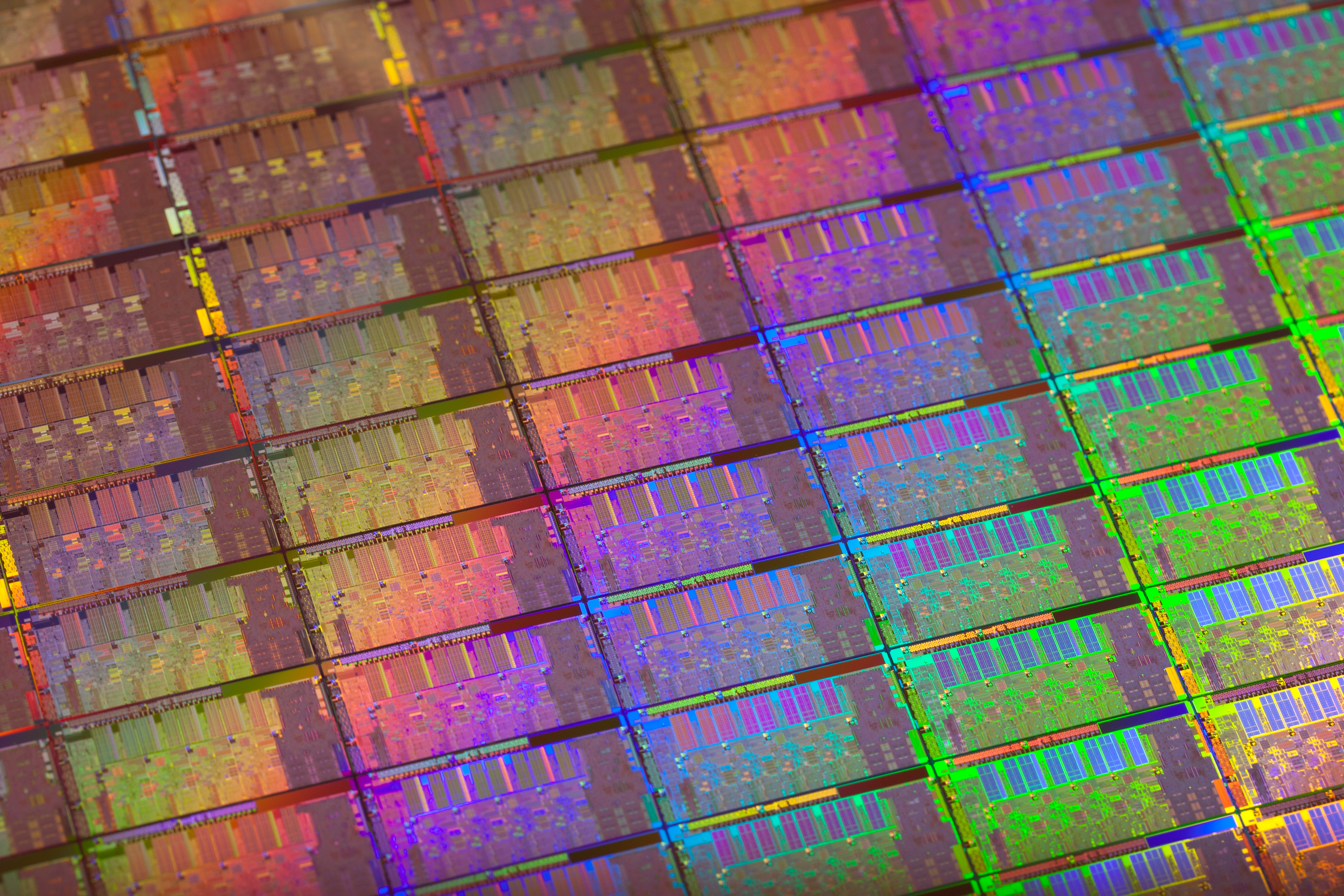
| 13:24, 30 July 2017 | sandy bridge whole wafer.png (file) |  |
5.87 MB | Intel {{intel|Sandy Bridge|l=arch}} wafer. Image by Intel. | 1 |
| 13:11, 30 July 2017 | sandy bridge partial wafer.png (file) |  |
7.52 MB | Intel's {{intel|Sandy Bridge|l=arch}} partial wafer. Image by Intel. * Annotated Version: File:sandy_bridge_partial_wafer_(annotated).png | 1 |
| 13:10, 30 July 2017 | sandy bridge partial wafer (annotated).png (file) | .png) |
5.39 MB | Intel's {{intel|Sandy Bridge|l=arch}} partial wafer. Annotated Version by WikiChip. * Original Version: File:sandy_bridge_partial_wafer.png | 1 |
| 13:05, 30 July 2017 | sandy bridge ucache.svg (file) |  |
27 KB | Intel {{intel|Sandy Bridge|l=arch}} ucache | 1 |
| 03:18, 29 July 2017 | sandy bridge decode.svg (file) |  |
26 KB | Intel {{intel|Sandy Bridge|l=arch}} decode stage | 1 |
| 17:51, 28 July 2017 | sandy bridge fetch.svg (file) |  |
15 KB | Intel's {{intel|Sandy Bridge|l=arch}} fetch. | 1 |
| 14:53, 20 July 2017 | ibm 14nm m2 cx.png (file) |  |
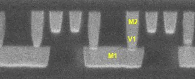
144 KB | IBM 14 nm process M2 cross-section. Image by IBM. | 1 |
| 14:52, 20 July 2017 | ibm 14nm m1 cx.png (file) |  |
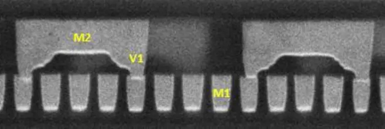
128 KB | IBM 14 nm process M1 cross-section. Image by IBM | 1 |
| 13:23, 20 July 2017 | 2015 InvestorMeeting Bill Holt WEB2.pdf (file) |  |
3.99 MB | * Advancing Moore's law * Bill Holt * Executive Vice President | 1 |
| 19:03, 16 July 2017 | broadwell avx turbo changes.png (file) |  |
538 KB | Intel {{intel|Broadwell|l=arch}} {{x86|AVX2}} turbo changes. From Intel's presentation. | 1 |
| 12:17, 16 July 2017 | skylake sp 4-way 3 upi.svg (file) |  |
437 KB | 3 | |
| 00:46, 15 July 2017 | skylake sp with hfi to carrier.png (file) |  |
1.49 MB | Intel {{intel|Skylake|l=arch}} SP with HFI to carrier. | 1 |
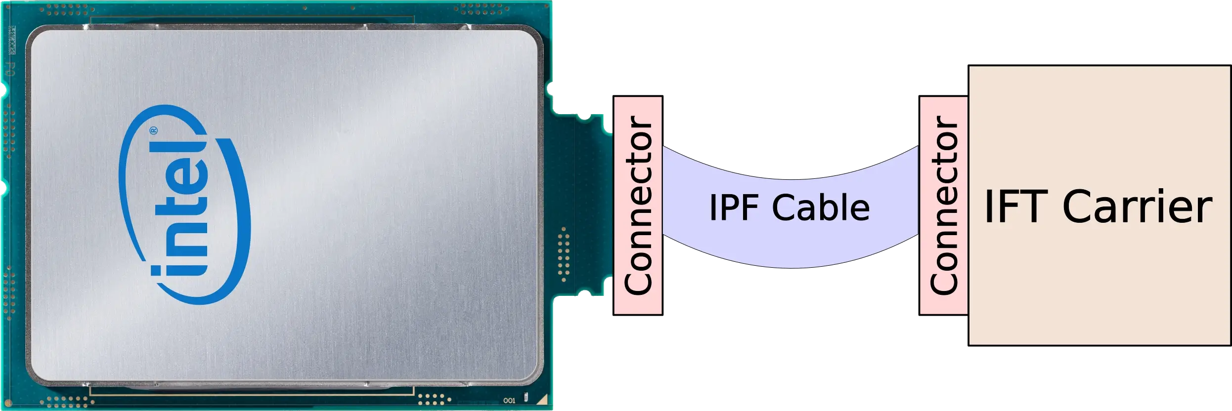
| 00:35, 15 July 2017 | omni-path ift carrier.png (file) |  |
807 KB | Intel {{intel|Omni-Path}} IFT carrier. As used in the {{intel|Knights Landing|l=arch}} and {{intel|Skylake|l=arch}} server configuration. Image by Intel. | 1 |
| 23:25, 14 July 2017 | skylake sp 8-way 3 upi.svg (file) |  |
436 KB | corrected mems more accurately | 3 |
| 23:25, 14 July 2017 | skylake sp 4-way 2 upi.svg (file) |  |
436 KB | corrected mems more accurately | 2 |
| 23:25, 14 July 2017 | skylake sp 2-way 3 upi.svg (file) | 436 KB | corrected mems more accurately | 2 | |
| 23:25, 14 July 2017 | skylake sp 2-way 2 upi.svg (file) | 436 KB | corrected mems more accurately | 2 | |
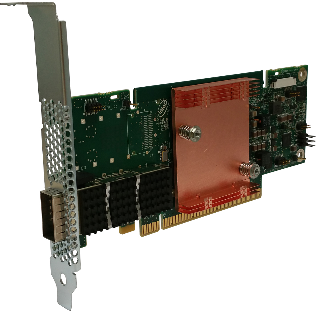
| 05:40, 14 July 2017 | skylake-sp (hfi).png (file) | .png) |
1.41 MB | Front view of the Intel {{intel|Skylake SP|l=core}} core based chip with integrated Host Fabric Interface (HFI). Image by Intel. | 1 |
| 02:00, 14 July 2017 | skylake sp xcc die config.png (file) |  |
385 KB | Die configuration of the {{intel|Skylake|l=arch}} SP XCC die. Image by Intel. | 1 |
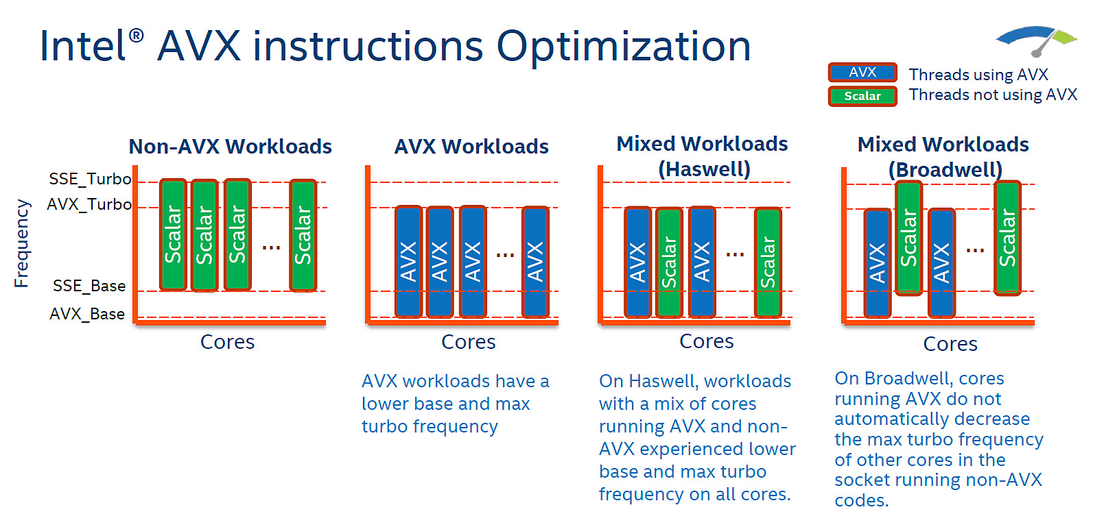
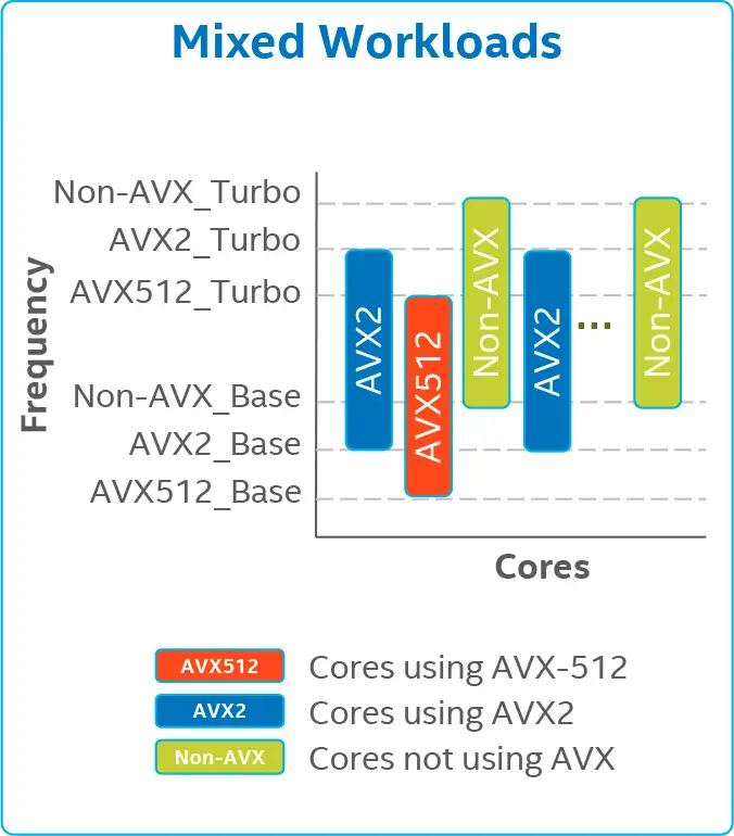
| 18:58, 13 July 2017 | mixed avx-normal workloads with avx512.png (file) |  |
191 KB | Intel's {{intel|Frequency Behavior}} from a slide by Intel | 1 |
| 06:28, 13 July 2017 | intel xeon skylake sp.jpg (file) |  |
2.26 MB | Intel {{intel|Skylake SP|l=core}} based processors. Image by Intel. | 1 |
| 06:18, 13 July 2017 | skylake scheduler server.svg (file) |  |
55 KB | Intel {{intel|Skylake|l=arch}} server scheduler | 1 |
| 06:02, 13 July 2017 | skylake server cache bandwidth.svg (file) |  |
10 KB | Intel {{intel|Skylake|l=arch}} server configuration cache bandwidth | 1 |
.png&action=edit&redlink=1)
First page |
Previous page |
Next page |
Last page |