-
WikiChip
WikiChip
-
Architectures
Popular x86
-
Intel
- Client
- Server
- Big Cores
- Small Cores
-
AMD
Popular ARM
-
ARM
- Server
- Big
- Little
-
Cavium
-
Samsung
-
-
Chips
Popular Families
-
Ampere
-
Apple
-
Cavium
-
HiSilicon
-
MediaTek
-
NXP
-
Qualcomm
-
Renesas
-
Samsung
-
From WikiChip
NNP-I 1300 - Intel Nervana
| Edit Values | |
 | |
| General Info | |
| Microarchitecture |
NNP-I 1300 is an inference neural processor designed by Intel Nervana and introduced in late 2019. Fabricated on Intel's 10 nm process based on the Spring Hill microarchitecture, the NNP-I 1300 comes in a PCIe Gen 3.0 accelerator card form factor with two NPU chips, each with all 24 ICEs enabled for a peak performance of 170 TOPS at a TDP of 75 W.
Facts about "NNP-I 1300 - Intel Nervana"
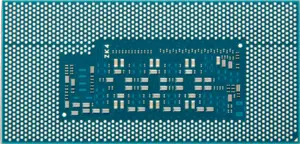
| back image |  + + |
| core count | 24 + |
| designer | Intel + |
| die area | 239 mm² (0.37 in², 2.39 cm², 239,000,000 µm²) + |
| family | NNP + |
| first announced | November 12, 2019 + |
| first launched | November 12, 2019 + |
| full page name | nervana/nnp/nnp-i 1300 + |
| has ecc memory support | true + |
| instance of | microprocessor + |
| ldate | November 12, 2019 + |
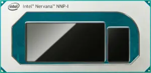
| main image |  + + |
| manufacturer | Intel + |
| market segment | Server + and Edge + |
| max memory bandwidth | 62.585 GiB/s (64,086.914 MiB/s, 67.2 GB/s, 67,200 MB/s, 0.0611 TiB/s, 0.0672 TB/s) + |
| microarchitecture | Spring Hill + |
| model number | NNP-I 1300 + |
| name | NNP-I 1300 + |
| peak integer ops (8-bit) | 170,000,000,000,000 OPS (170,000,000,000 KOPS, 170,000,000 MOPS, 170,000 GOPS, 170 TOPS, 0.17 POPS, 1.7e-4 EOPS, 1.7e-7 ZOPS) + |
| process | 10 nm (0.01 μm, 1.0e-5 mm) + |
| series | NNP-I + |
| supported memory type | LPDDR4X-4200 + |
| tdp | 75 W (75,000 mW, 0.101 hp, 0.075 kW) + |
| technology | CMOS + |
| transistor count | 8,500,000,000 + |