From WikiChip
z15 - Microarchitectures - IBM
| Edit Values | |
| z15 µarch | |
| General Info | |
| Arch Type | CPU |
| Designer | IBM |
| Manufacturer | GlobalFoundries |
| Introduction | September 12, 2019 |
| Process | 14 nm |
| Core Configs | 12 |
| Pipeline | |
| Type | Superscalar, Pipelined |
| OoOE | Yes |
| Speculative | Yes |
| Reg Renaming | Yes |
| Instructions | |
| ISA | z/Architecture |
| Cache | |
| L1I Cache | 128 KiB/core 8-way set associative |
| L1D Cache | 128 KiB/core 8-way set associative |
| L3 Cache | 256 MiB/chip 32-way set associative |
| L4 Cache | 960 MiB/drawer 60-way set associative |
| Succession | |
z15 is the successor to the z14, a 14 nm z/Architecture mainframe microarchitecture designed by IBM and introduced in 2019.
Contents
Process Technology
IBM fabricates its z15 microprocessors and system controllers on GlobalFoundries's 14 nm (14HP) FinFET Silicon-On-Insulator (SOI) process featuring highly-dense deep trench structures used for high-density eDRAM.
Release Dates
The z15 was launched by IBM on September 12, 2019. General availability of the z15 mainframe started September 23.
Architecture
Key changes from z14
- Scalability
- Up to 190-way multiprocessing (from 170-way)
- Less CPs per drawer (4, down from 6)
- Less CPs per logical cluster (2, down from 3)
- 1 more drawer (5, up from 4)
- Central Processor (CP)
- 2 more cores (12, up from 10)
- Core
- 10-13% higher IPC (IBM claim)
- Front-end
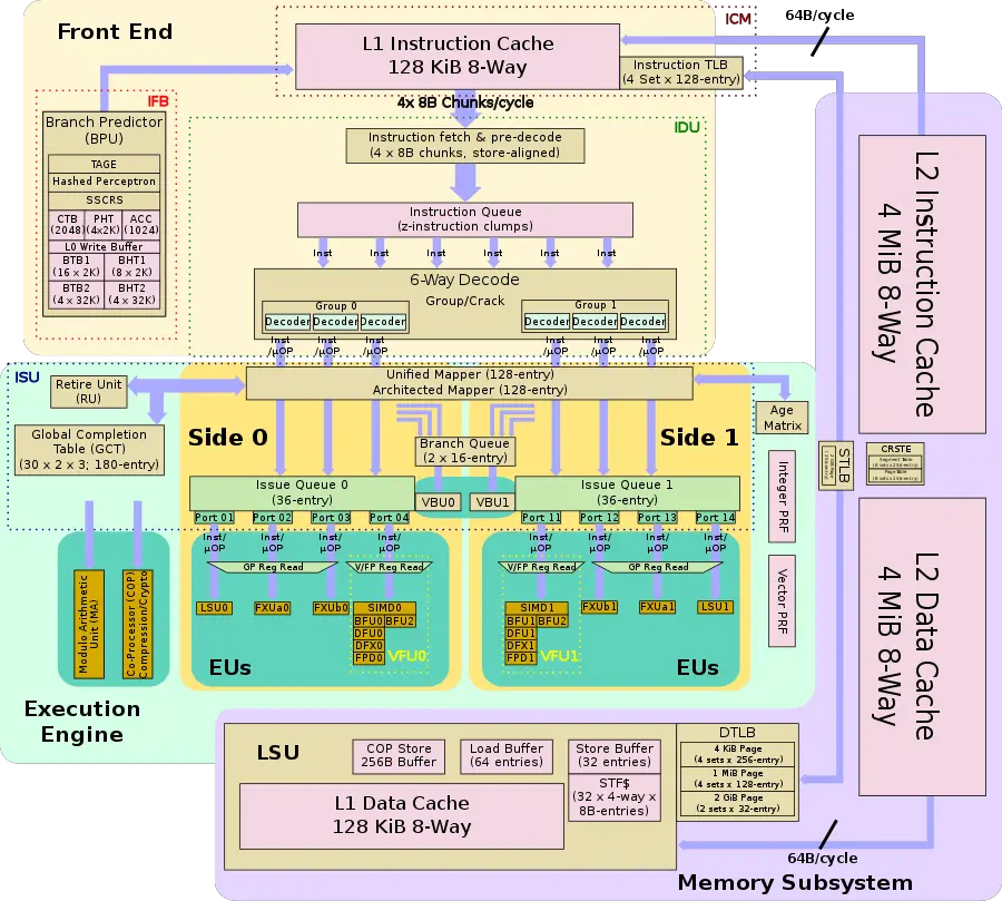
- Improved branch predictor
- New TAGE predictor
- BTB pre-buffer (BTBp) replaced by a simpler write buffer
- single double-bandwidth port (two independentread ports)
- 2x larger L1 BTB (8 sets of 2K rows, up from 4 sets of 2K rows)
- Improved branch predictor
- Back-end
- Larger GCT (60 groups, up from 48 groups)
- Wider retire (12 instructions/cycle, up from 10)
- Larger Issue Queues (2 x 36-entry, up from 2 x 30-entry)
- 2x larger mapper (128-entry, up from 64-entry)
- Larger integer physical register files (???, up from 120 entries)
- Larger vector physical register files (???, up from 127 entries)
- Larger GCT (60 groups, up from 48 groups)
- Execution engine
- Wider execute (12 instructions/cycle, up from 10)
- New Modulo Arithmetic (MA) unit
- Memory subsystem
- 2x larger L2 instruction cache (4 MiB, up from 2 MiB)
- 2x larger 2 GiB pages STLB (256-entry, up from 64 entries)
- Shared L3
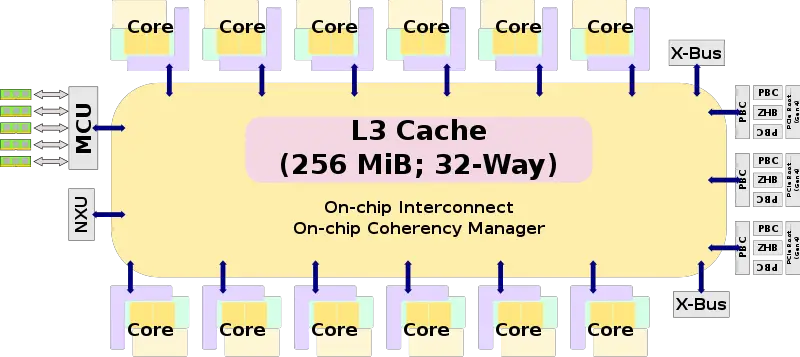
- 2x larger L3 (256 MiB, up from 128 MiB)
- I/O
- GX Bus removed
- X Bus removed (2 interface, down from 3)
- New PCIe Gen interface (3 interfaces, up from 2)
- Memory
- Larger memory support (40 TiB, up from 32 TiB)
- New integration
- Nest Acceleration Unit (NXU)
- System Controller (SC)
- 1.4x Larger L4 cache (960 MiB, up from 672 MiB)
- Non-exclusive (from inclusive)
- 1.4x Larger L4 cache (960 MiB, up from 672 MiB)
Block Diagram
CP Chip
Individual core
Memory Hierarchy
The z15 features a memory structure very similar to the z14.
- Cache:
- L1 instruction cache
- 128 KiB, 8-way set associative
- 64 sets, 256 B line size
- L1 data cache
- 128 KiB, 8-way set associative
- 64 sets, 256 B line size
- L2 instruction cache
- 4 MiB, 8-way set associative
- 2K sets, 256 B line size
- L2 data cache
- 4 MiB, 8-way set associative
- 2K sets, 256 B line size
- L3 cache
- 256 MiB, 32-way set associative
- 32K sets, 256 B line size
- L4 cache (off-chip, on the SC chip)
- 960 MiB, 40-way set associative
- 64K sets, 256 B line size
- Non-exclusive (almost always inclusive, but not strictly)
- System Memory
- Up to 40 TiB
- Up 5 DIMMs (one DIMM per channel)
- 5th DIMM for Redundant Array of Independent Memory (RAIM) (Note: No non-RAIM option)
- 32, 64, 128, 256 and 512 GiB DIMMs
- L1 instruction cache
- TLBs:
- ITLB
- 4 sets x 128 entries
- DTLB
- 4 KiB pages
- 4 sets x 256 entries
- 1 MiB pages
- 4 sets x 128 entries
- 2 GiB pages
- 2 sets x 32 entries
- 4 KiB pages
- STLB
- 4 KiB pages
- 6K entries
- 2 GiB pages
- 256 entries
- Segment Table
- 8 sets x 256 entries
- Page Table
- 8 sets x 256 entries
- 4 KiB pages
- ITLB
Overview
Mainframe
| This section is empty; you can help add the missing info by editing this page. |
System
| This section is empty; you can help add the missing info by editing this page. |
Drawer
| This section is empty; you can help add the missing info by editing this page. |
Central Processor
| This section is empty; you can help add the missing info by editing this page. |
Core
| This section is empty; you can help add the missing info by editing this page. |
Die
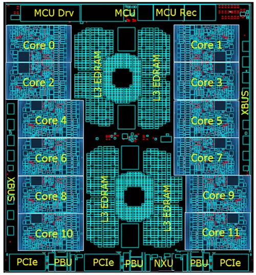
Central Processor (CP) Chip
- 14HP FinFET on SOI
- 17 metal layers
- 9,200,000,000 transistors
- 5.2 GHz
- 12 cores
- Die size
- 25.3 mm x 27.5 mm
- 695.75 mm²
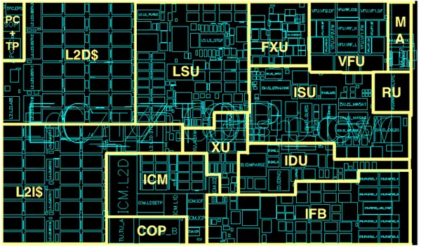
Core
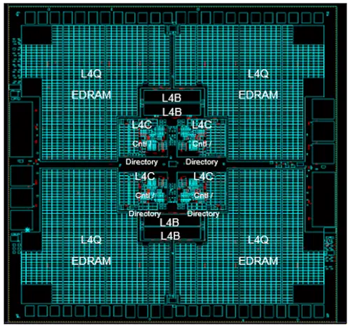
System Controller (SC) Chip
- 14HP FinFET on SOI
- 17 metal layers
- 9,700,000,000 billion transistors (note that this number, from the technical document, is likely incorrect as it's the same number as the z14)
- 960 MiB shared eDRAM L4 cache.
- Die size
- 25.3 mm x 27.5 mm
- 695.75 mm²
Facts about "z15 - Microarchitectures - IBM"
| codename | z15 + |
| core count | 12 + |
| designer | IBM + |
| first launched | September 12, 2019 + |
| full page name | ibm/microarchitectures/z15 + |
| instance of | microarchitecture + |
| instruction set architecture | z/Architecture + |
| manufacturer | GlobalFoundries + |
| microarchitecture type | CPU + |
| name | z15 + |
| process | 14 nm (0.014 μm, 1.4e-5 mm) + |
