| Edit Values | |
| Mongoose 4 µarch | |
| General Info | |
| Arch Type | CPU |
| Designer | Samsung |
| Manufacturer | Samsung |
| Introduction | 2019 |
| Process | 8 nm |
| Core Configs | 4 |
| Pipeline | |
| Type | Superscalar, Superpipeline |
| OoOE | Yes |
| Speculative | Yes |
| Reg Renaming | Yes |
| Stages | 16 |
| Decode | 6-way |
| Instructions | |
| ISA | ARMv8.2 |
| Cache | |
| L1I Cache | 64 KiB/core 4-way set associative |
| L1D Cache | 64 KiB/core 8-way set associative |
| L2 Cache | 512 KiB/core 8-way set associative |
| L3 Cache | 4 MiB/cluster 16-way set associative |
| Succession | |
Exynos Mongoose 4 (M4) is the successor to the Mongoose 3, an 8 nm ARM microarchitecture designed by Samsung for their consumer electronics.
Contents
Process Technology
The M4 is fabricated on Samsung's 8 nm process (8LPP).
Compiler support
| Compiler | Arch-Specific | Arch-Favorable |
|---|---|---|
| GCC | -mcpu=exynos-m4 |
-mtune=exynos-m4
|
| LLVM | -mcpu=exynos-m4 |
-mtune=exynos-m4
|
Architecture
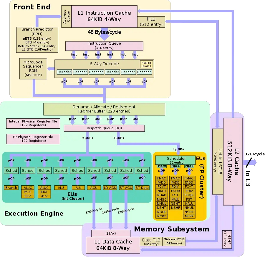
The M4 is an incremental microarchitecture that brought a die shrink and minor enhancements.
Key changes from M3
- 8 nm process (from 10 nm)
- ARMv8.2 (from ARMv8)
- Support for full FP16 scalar extension
- Suppot for integer dot product extension
- Front end
- Larger instruction queue (48 entries, up from 40)
- Back end
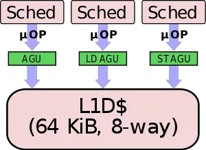
- LSU executiion units reorganized
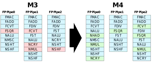
- Floating-point execution units reorganized
This list is incomplete; you can help by expanding it.
Block Diagram
Individual Core
Memory Hierarchy
- Cache
- L1I Cache
- 64 KiB, 4-way set associative
- 128 B line size
- per core
- Parity-protected
- 64 KiB, 4-way set associative
- L1D Cache
- 64 KiB, 8-way set associative
- 64 B line size
- per core
- 4 cycles for fastest load-to-use
- 32 B/cycle load bandwidth
- 16 B/cycle store bandwidth
- 64 KiB, 8-way set associative
- L2 Cache
- 512 KiB, 8-way set associative
- Inclusive of L1
- 12 cycles latency
- 32 B/cycle bandwidth
- L3 Cache
- 4 MiB, 16-way set associative
- 1 MiB slice/core
- Exlusive of L2
- ~37-cycle typical (NUCA)
- 4 MiB, 16-way set associative
- BIU
- 80 outstanding transactions
- L1I Cache
The M4 TLB consists of dedicated L1 TLB for instruction cache (ITLB) and another one for data cache (DTLB). Additionally, there is a unified L2 TLB (STLB).
- TLBs
- ITLB
- 512-entry
- DTLB
- 32-entry
- 512-entry Mid-level DTLB
- STLB
- 4,096-entry
- Per core
- ITLB
- BPU
- 4K-entry main BTB
- 128-entry µBTB
- 64-entry return stack
- 16K-entry L2 BTB
Core
The core of the M4 is largely the same as M3. A number of buffers have been enlarged and some of the execution units have been reorganized.
Execution engine
Floating-point cluster
The execution units on the M4 have been reorganized. In total, three new units were also added - a second FP square root unit, a second vector multiplication unit, and a new horizontal vector arithmetic unit.
Memory subsystem
A minor enhancement was made to the M4 memory subsystem. In the M3, there were three AGUs - two dedicated Load AGUs and a single dedicated Store AUG. In the M4, Samsung changed one of the dedicated Load AGUs into a generic AGU capable of handling both loads and stores. In other words, the M4 can now schedule both load and store µOPs on two ports.
All M3 Processors
| List of M4-based Processors | |||||||
|---|---|---|---|---|---|---|---|
| Main processor | Integrated Graphics | ||||||
| Model | Family | Launched | Arch | Cores | Frequency | GPU | Frequency |
| Count: 0 | |||||||
Bibliography
- LLVM: lib/Target/AArch64/AArch64SchedExynosM4.td
| codename | Cheetah + |
| core count | 4 + |
| designer | Samsung + |
| first launched | 2019 + |
| full page name | samsung/microarchitectures/m4 + |
| instance of | microarchitecture + |
| instruction set architecture | ARMv8.2 + |
| manufacturer | Samsung + |
| microarchitecture type | CPU + |
| name | Cheetah + |
| pipeline stages | 16 + |
| process | 8 nm (0.008 μm, 8.0e-6 mm) + |


