From WikiChip
NNP-T 1300 - Intel Nervana
| Edit Values | |
| NNP-T 1300 | |
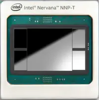 | |
| NPU with 4 HBM2 stacks | |
| General Info | |
| Designer | Intel |
| Manufacturer | TSMC |
| Model Number | NNP-T 1300 |
| Market | Server |
| Introduction | November 12, 2019 (announced) November 12, 2019 (launched) |
| Shop | Amazon |
| General Specs | |
| Family | NNP |
| Series | NNP-T |
| Frequency | 950 MHz |
| Microarchitecture | |
| Microarchitecture | Spring Crest |
| Process | 16 nm |
| Transistors | 27,000,000,000 |
| Technology | CMOS |
| Die | 680 mm² |
| Cores | 22 |
| Max Memory | 32 GiB |
| Multiprocessing | |
| Interconnect | InterChip Link |
| Interconnect Links | 16 |
| Interconnect Rate | 28 GT/s |
| Electrical | |
| Power dissipation | 150 W |
| TDP | 300 W |
| Packaging | |
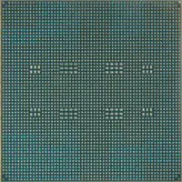
| Package | FCBGA-3325 (FCBGA) |
| Dimension | 60 mm × 60 mm |
| Contacts | 3325 |
 | |
NNP-T 1300 is a training neural processor designed by Intel Nervana and introduced in late 2019. Fabricated on TSMC 16 nm process based on the Spring Crest microarchitecture, the NNP-T 1300 has 22 TPCs along with 55 MiB of scratchpad memory and operates at up to 950 MHz. This chip comes in a PCIe 4.0 accelerator card form factor and incorporates 32 GiB of HBM2 memory. This NPU exposes 16 inter-chip links for scale-out capabilities.
Contents
Peak Performance
The NNP-T 1300 has a peak performance of 93.39 TFLOPS93,390,000,000,000 FLOPS
93,390,000,000 KFLOPS
93,390,000 MFLOPS
93,390 GFLOPS
0.0934 PFLOPS
(bfloat16).
93,390,000,000 KFLOPS
93,390,000 MFLOPS
93,390 GFLOPS
0.0934 PFLOPS
Cache
- Main article: Spring Crest § Cache
- 55 MiB of tightly-coupled scratchpad memory
- 22 x 2.5 MiB/core
Memory controller
|
Integrated Memory Controller
|
||||||||||||
|
||||||||||||
Interconnect Topology
The NNP-T 1300 comes in a dual-slot standard PCIe 4.0 card which enables support for only the ring topology. Chips are interconnected using the 16 available inter-chip links.
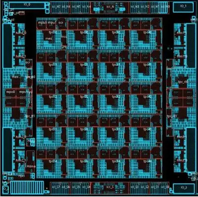
Die
- Main article: Spring Crest § Die
- 27,000,000,000 transistors
- 680 mm² die size
Product Brief
Facts about "NNP-T 1300 - Intel Nervana"
| back image |  + + |
| base frequency | 950 MHz (0.95 GHz, 950,000 kHz) + |
| core count | 22 + |
| designer | Intel + |
| die area | 680 mm² (1.054 in², 6.8 cm², 680,000,000 µm²) + |
| family | NNP + |
| first announced | November 12, 2019 + |
| first launched | November 12, 2019 + |
| full page name | nervana/nnp/nnp-t 1300 + |
| has ecc memory support | true + |
| instance of | microprocessor + |
| ldate | November 12, 2019 + |
| main image | 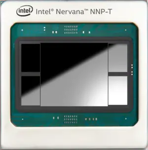 + + |
| main image caption | NPU with 4 HBM2 stacks + |
| manufacturer | TSMC + |
| market segment | Server + |
| max memory | 32,768 MiB (33,554,432 KiB, 34,359,738,368 B, 32 GiB, 0.0313 TiB) + |
| max memory bandwidth | 1,144.409 GiB/s (1,171,875 MiB/s, 1,228.8 GB/s, 1,228,800 MB/s, 1.118 TiB/s, 1.229 TB/s) + |
| max memory channels | 32 + |
| microarchitecture | Spring Crest + |
| model number | NNP-T 1300 + |
| name | NNP-T 1300 + |
| package | FCBGA-3325 + |
| peak integer ops (8-bit) | 50,000,000,000,000 OPS (50,000,000,000 KOPS, 50,000,000 MOPS, 50,000 GOPS, 50 TOPS, 0.05 POPS, 5.0e-5 EOPS, 5.0e-8 ZOPS) + |
| power dissipation | 150 W (150,000 mW, 0.201 hp, 0.15 kW) + |
| process | 16 nm (0.016 μm, 1.6e-5 mm) + |
| series | NNP-T + |
| smp interconnect | InterChip Link + |
| smp interconnect links | 16 + |
| smp interconnect rate | 28 GT/s + |
| supported memory type | HBM2-2400 + |
| tdp | 300 W (300,000 mW, 0.402 hp, 0.3 kW) + |
| technology | CMOS + |
| transistor count | 27,000,000,000 + |
